Specifying transceivers for serial protocols
FPGA-based transceivers with dynamic reconfiguration deliver an elegant solution for multirate and multiprotocol serial I/O
BY JOEL MARTINEZ, SRIDHAR KRISHNAMURTHY, and VENKAT YADAVALLI
Altera, San Jose, CA
http://www.altera.com
The rapid adoption of high-speed serial interconnect in recent years have posed new challenges to design engineers. Many embedded systems engineers are facing designs with PCIe and Serial Rapid I/O, and this trend will continue.
Design engineers must keep up with system bandwidth demands while maintaining compatibility with legacy line cards and attempting to support next-generation higher-bandwidth systems. The data rates of serial protocols are doubling and quadrupling, with PCI Express a prime example. Before the ink dried on the Gen 1.0 2.5 Gbits/s specification, work was underway on the Gen 2.0 specification for 5.0 Gbits/s serial data rate. Now, the standards body is defining 8.0 Gbits/s Gen 3.0.
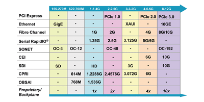
Some of today’s more popular serial protocols are summarized in Table 1 . While many of these protocols share common physical layer and data link layers—differences appear in the upper layers of the protocol stack. The upper layers are geared to address specific needs of the application.
Increasing data rates
PCI Express has realized broad adoption across various market segments due to the ubiquity of PCs. Ethernet was targeted for datacom, Fibre Channel for storage; Serial Rapid I/O for signal processing; SONET and CEI for datacom/telecom; SDI for broadcast; CPRI and OBSAI for wireless applications.
The common thread with these protocols is that all are offered with increasing data rates. The transceivers selected for an application should address future data rate requirements because plans will undoubtedly call for an increase in speeds.
Additionally, it is important to verify standards compliance and availability of characterization data of the transceiver. Selecting robust transceivers can save many potential problems in the future.

Table 1. Summary of serial protocols, many of which share a common physical layer
FPGAs with transceivers combined with dynamic reconfiguration delivers an elegant solution for multirate and/or multiprotocol serial applications. With dynamic reconfiguration, users may optimize signal integrity, change data rates and switch protocols at run time. Users may reconfigure a channel without interrupting other serial channels, and avoid costly network or system down-times.
A user may also dynamically reconfigure transmit output voltage amplitude and pre-emphasis settings, or receive equalizer settings, to optimize signal integrity for backplane and cable applications. The signal integrity of the transceiver must be optimized for each data rate and protocol in order to meet standards for jitter generation and jitter tolerance.
One transceiver can service all protocols
In some cases, engineers face the challenge of designing a system requiring multiple protocols—such as optical network interface cards that support Fibre Channel, SONET, and GbE. Supporting FC1G, FC2G, FC4G, OC3, OC12, OC48, and GbE could entail designing and stocking seven different boards that using different ASSPs to implement the PHY, PCS, data link, and MAC layers.
Why not design a single optical network interface card that supports all of these protocols and data rates, trading seven BOMs for one? End users would have the flexibility to configure an optical channel to any of the seven protocols at run time, providing ultimate flexibility at the fraction of the cost of seven boards.

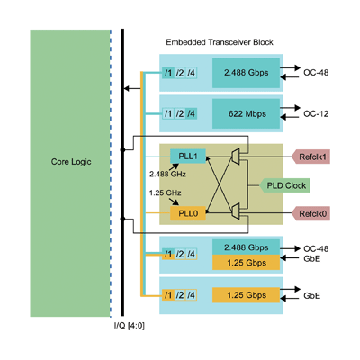
Fig. 1. A single FPGA-based transceiver supports multiple protocols.
In Fig. 1 , each of the four channels in the transceiver block can support multiple data rates and protocols. In this example, the transceiver block receives two reference clocks, one for GbE (125 MHz) and the other for SONET rates (311 or 622 MHz).
The reference clocks are multiplied up as they pass through the PLLs. Each transmitter channel can be dynamically configured to select one of two clock domains for each channel during run time. The dedicated local dividers (1/, /2, and /4) enable the use of the PLL clock frequency to support different data rates within the same protocol.
For this example, the user can switch between OC12 and OC48 by using the PLL1 clock output and dynamically reconfiguring the local divider values. The transceiver offers capabilities to reconfigure the transceiver PCS blocks that enable users to use the embedded PCS blocks for specific protocols. By reconfiguring the PCS block, the user can dynamically enable the 8b/10b encoder and the clock rate compensation FIFO in the PCS block when switching to GbE protocol. Each receiver channel contains dedicated clock and data recovery (CDR), local dividers, and PCS blocks that provide full control to the user for reconfiguring the receiver data path in support of multiple protocols and data rates.

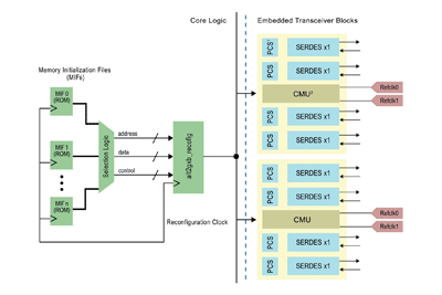
Fig. 2. A typical dynamic reconfiguration block.
Using Quartus II FPGA software simplifies channel reconfiguration by generating memory initialization files (MIF) for each protocol. MIF files include PLL, PMA, and PMS settings required to correctly configure a transceiver channel for a given protocol. Figure 2 illustrates the dynamic reconfiguration block (alt2gxb_reconfig) that writes unique MIFs containing transceiver settings for a specific protocol. There will be three unique MIFs for this example, one each for OC48, OC12, and GbE. A single reconfiguration block controls all the transceiver channels and PLLs that further simplifies the design.

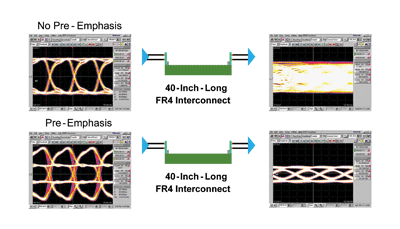
Fig. 3. Eye diagrams show the circuits signal integrity at 6.375 Gbits/s.
User’s may also dynamically change transmit amplitude, pre-emphasis, and equalization settings to optimize signal integrity. ■
For more on FPGA-based transceivers, visit http://electronicproducts-com-develop.go-vip.net/digital.asp.
Advertisement
Learn more about Altera


