Given the limited number of DC/DC converters that can efficiently support output currents greater than 30 A, design engineers have primarily relied on multiphase buck controllers with external field-effect transistors (FETs) for high-current applications.
New point-of-load DC/DC buck converters with integrated metal-oxide semiconductor FETs (MOSFETs) can achieve high output currents when interconnected with multiple converters, otherwise known as stacking. Stacking converters enable designers to harness the benefits of FET integration in high-current applications.
In this article, I’ll use WEBENCH Power Designer to compare and contrast one design — using the Texas Instruments (TI) dual-phase TPS40425 DC/DC controller with external power stages — with a second design using two 40-A TPS546D24A stacked integrated FET DC/DC converters, also from TI. WEBENCH Power Designer is an end-to-end online design tool that creates customized power supply circuits based on the user’s requirements.
All designs referenced in this article, as well as the data collected from said designs, will be gathered from the WEBENCH tool. Both the controller- and converter-based designs have the same input voltage (12 V), output voltage (1 V), switching frequency (550 kHz), and output current (50 A). I’ll compare the resulting size, thermal dissipation, efficiency, and cost; discuss the advantages of both device types; and highlight why one design architecture might have an advantage in certain design scenarios.
Power density
Power density is defined as a measure of power output per unit volume. A higher power density is highly valuable to engineers looking to create designs that can deliver higher currents in a smaller area. For comparing area, the WEBENCH Power Designer tool’s size-optimization setting is applied to both designs. WEBENCH defines design area as the sum of the footprint sizes of the integrated circuits (ICs), all external components, and all necessary keep-out areas for the components. Stackable buck converters have a distinct advantage over multiphase buck controllers when minimal area and high power density are priorities.
For example, the TPS40425 controller design yields a total area of 916 mm2, while the same optimization settings for two stacked TPS546D24A converters yields a total area of 802 mm2. This 14.2% area reduction is because the two converters have integrated MOSFETs. In the controller design, two external power stages have a footprint of 56 mm2 each, while the converter fully integrates the equivalent FETs within the IC.
When stacking converters to achieve higher currents, the size advantage of the converter design begins to diminish because each individual converter integrates both a controller and a MOSFET. In other words, for each newly stacked converter, there is a controller taking up more board space. For a controller, you only need to add more power stages while keeping one controller IC. Therefore, adding more power stages to a controller design requires less board space than stacking converters in a converter design.
It is not currently possible to stack more than four converters, which limits the amount of current that the stackable converters can output. Multiphase controller designs with external power stages can output higher currents.
There is a point at which the TPS546D24A converter design begins to yield a bigger area than a controller design. A single TPS546D24A converter operating at its maximum output current of 40 A and switching frequency of 550 kHz has an approximate design area of 585 mm2. The design area for two or more stacked converters is estimated to scale proportionally with the area of one converter. For example, in a design with two converters stacked together, the design area would be approximately 2 × (585 mm2) = 1,170 mm2.
Stacking as many as four TPS546D24A converters will produce a total output current of 160 A, but the TPS40425 controller can reach a maximum load current of only 80 A. Instead, let’s compare the size of the TPS546D24A converter at each stack quantity with the six-phase TPS53667 controller, which has a maximum output current of 160 A.
Tables 1 and 2 show the estimated required solution size at each quantity of the stackable converter compared with the required solution size of a controller that outputs an equivalent output current.
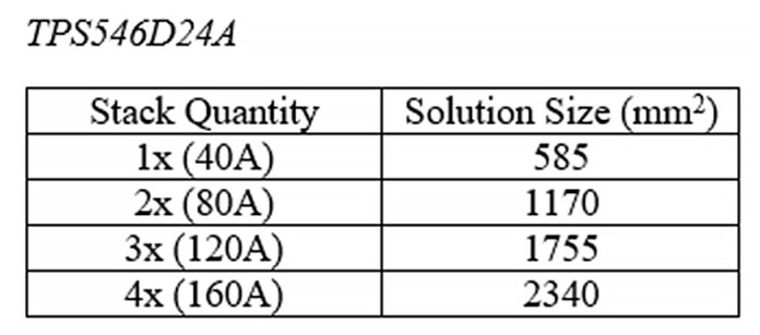
Table 1: Solution size of TPS546D24A converters at various stack quantities (Source: Texas Instruments Inc.)
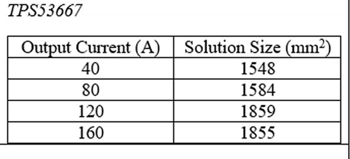
Table 2: Solution size of the TPS53667 controllers at each equivalent output current (Source: Texas Instruments Inc.)
The size advantage of stacked converters diminishes significantly when stacking three converters, with a larger design area than the controller design when stacking four converters. I have made a number of approximations that affect the exact footprint measurements for this comparison. The converter design assumes the inclusion of a few mode-select resistors with every stacked converter IC. In practice, those resistors would, at most, be required for only one converter in a stacked design.
The TPS53667 controller uses six power stages, compared with the four total power stages integrated in the TPS546D24A converter. Ideally, the four-stacked-converter design would directly compare with a four-phase controller design that requires only four power stages instead of six, which would yield a smaller size. The fact that the converter design is larger than a six-phase controller design shows the extent at which size is compromised at greater stack quantities. Despite these approximations, you can expect the stackable converter design to lose its size advantage against the multiphase controllers when stacked four times.
Efficiency
Efficiency is largely reliant on the chosen FET or power stage located on the switch node, regardless of whether it is integrated or located externally. When comparing the efficiency of the TPS546D24A stackable converter design with the TPS40425 multiphase buck controller design using the CSD95372BQ5M external power stage, you can see that the efficiency at 50 A of both designs is quite similar: 89.5% for the converter and 89.9% for the controller. The efficiency verus load current graph in Figure 1 shows that the controller design tends to have better efficiency overall until an approximate 55-A load current.
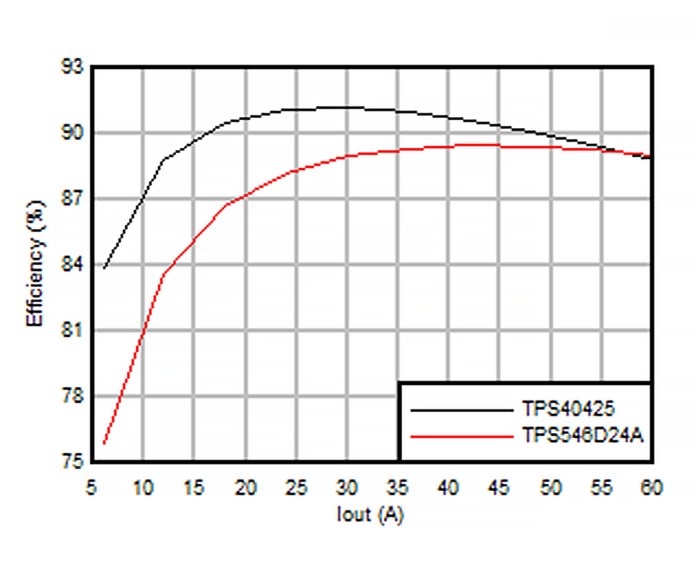
Figure 1: Efficiency vs. load current at Fsw = 500 kHz (Source: Texas Instruments Inc.)
The advantage of the CSD95372AQ5M external power stage is that its recommended maximum operating switching frequency is 2,000 kHz, so choosing a higher switching frequency requires less of a compromise. As you can see in Figure 2, the external power stage can sustain higher efficiency at a higher switching frequency than the integrated FET in the converter. If your design does not need to operate at higher switching frequencies, you can swap out the power stage for the CSD95327BQ5M, which has higher efficiency but at a higher cost and a lower tolerance for input voltage noise. The freedom for designers to choose the best external power stage for their design is an advantage when optimizing efficiency is a priority.
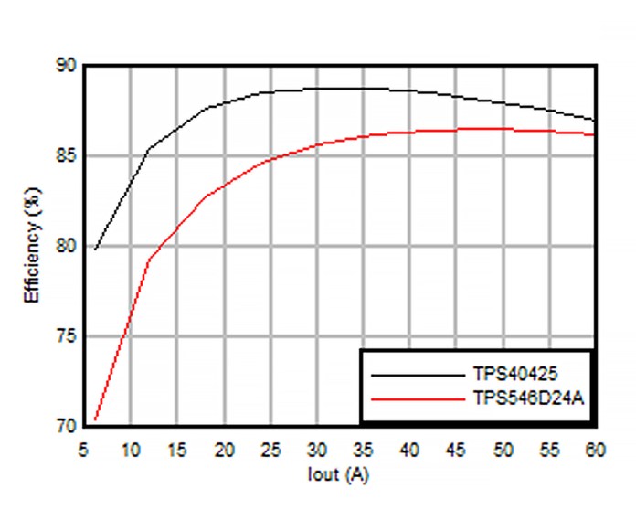
Figure 2: Efficiency vs. load current at Fsw = 900 kHz (Source: Texas Instruments Inc.)
Power loss directly affects efficiency. A significant source of power loss in synchronous buck converters comes from MOSFET loss, which is made up of both conduction loss and switching loss. Conduction loss is determined by the on-resistances of the MOSFETs and the transistor’s root-mean-square current. Switching loss comprises several parts: MOSFET switching loss (high side and low side), MOSFET gate-drive loss, low-side body diode loss, and MOSFET output capacitance loss. The chosen input parameters of a specific application (such as the input voltage, output voltage, output current, and switching frequency) influence the magnitude of both losses. External power stages in a controller design enable designers to choose a power stage that minimizes total power loss and maximizes efficiency in their specific application. Converters do not provide this freedom.
Unfortunately, it is not possible to optimize the integrated FETs in a converter further, which prevents you from reaching the same efficiency as an efficiency-optimized controller design. You could make a case for the ease of use of the converter design, however. The time invested in minimizing the power loss in a controller design may not be worth the marginal benefit in efficiency.
Thermal dissipation
Thermal dissipation is a form of printed-circuit–board (PCB) power loss that affects a design’s efficiency. Effective heat dissipation maximizes the copper area that conducts heat on the PCB. In a DC/DC step-down buck controller and converter layout, the source of heat generation comes from both the multiphase controller and the power stage. A design that yields more power density tends to have worse thermal dissipation.
Because the TPS546D24A converter integrates the power stage and controller, the source of heat generation comes from just the two converter ICs, which have a footprint of 126 mm2. The controller design generates heat from the main controller IC and the two external power stages, which have a footprint of 178 mm2. The controller design can dissipate heat 41% better than the converter design, so theoretically, controller designs tend to have better thermal performance.
Design cost
Let’s use the cost-optimization feature in WEBENCH Power Designer to compare the cost and size of each design at both optimization settings and generate bill-of-materials (BOM) costs from WEBENCH Power Designer.
When optimizing for cost, the BOM cost of the TPS546D24A converter design is lower than the BOM cost of the TPS40425 controller design. When optimizing for size, the TPS546D24A converter design has a solution size of 802 mm2 but at a $36.32 total BOM cost. The size-optimized design requires small-input bulk capacitors that account for $20.52, or over 50% of the total BOM cost. If minimizing cost is the greatest priority, you can swap out the bulk capacitors to a lower-cost option but with a higher design footprint.
Table 3 examines the difference between a design optimized for BOM cost and one optimized for size.
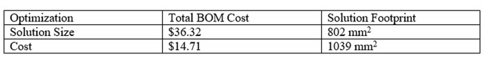
Table 3: Comparing BOM cost and solution size in a TPS546D24A converter design (Source: Texas Instruments Inc.)
Optimizing for cost enables a 59% BOM reduction but with a tradeoff of a 29% size increase. Whether this tradeoff is worth it depends on the application, but it is clear that a cost-optimized design is closer to a more balanced design than a size-optimized one.
For the TPS40425 controller design, as shown in Table 4, the total BOM cost includes the external power stages required.
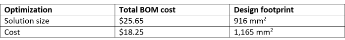
Table 4: Comparing BOM cost and solution size in the TPS40425 controller design (Source: Texas Instruments Inc.)
The cost reduction in this case comes from using lower-cost input capacitors that have a larger footprint. Because the controller design doesn’t require any bulk capacitors, there is less of a drastic difference in cost and footprint between the two optimizations. The size-optimized controller design costs 29% less than the converter design, although it is 14% larger. This is important because, for example, if your design is cost-sensitive and does not require the absolute minimal size, you may choose to opt for the size-optimized controller design rather than the more expensive converter design. The cost-optimized converter design offers a more balanced solution if you can tolerate a footprint >1,000 mm2, yielding both a cheaper total BOM cost and a smaller footprint than the cost-optimized controller design.
Procurement is also a factor when considering costs. Stackable converters simplify the procurement process because the integration of the power stage means that designers have to keep inventory for only one IC, rather than for an IC and its power stages. Mass procurement for one device can enable lower pricing at higher volumes even further, although the difference may not be as significant. The advantage that controllers have in procurement lies in the wide variety of vendors that supply power stages, FETs, and drivers.
Conclusion
Overall, stackable converters typically enable smaller sizes, which are less compromised even when optimizing for cost. Multiphase buck controllers provide better thermal dissipation and efficiency while giving designers freedom to position and select their own power stages. Using converters in wired networking and wireless infrastructure applications makes minimizing cost and size a priority. Multiphase controllers can be a good fit when you need high efficiency and superior thermal performance, or if your design requires very high currents.
Advertisement
Learn more about Texas Instruments


