At this week's IEEE International Electron Devices Meeting (IEDM) in San Francisco, CA, a Stanford team led by Subhasish Mitra, a Stanford associate professor of electrical engineering and of computer science, and H. S. Philip Wong, the Williard R. and Inez Kerr Bell Professor in Stanford's School of Engineering, described how to build “high-rise” chips that could significantly outperform current configurations. The work was done in collaboration with Professors Krishna Saraswat and Yoshio Nishi of Stanford University.
“This research is at an early stage, but our design and fabrication techniques are scalable,” Mitra said. “With further development this architecture could lead to computing performance that is much, much greater than anything available today.” “Paradigm shift is an overused concept, but here it is appropriate,” Wong said. “With this new architecture, electronics manufacturers could put the power of a supercomputer in your hand.”
The Stanford approach would end dataflow logjams by building layers of logic atop layers of memory to create a tightly interconnected high-rise chip. Many thousands of nanoscale electronic “elevators” would move data between the layers much faster, using less electricity, than the bottleneck-prone wires connecting single-story logic and memory chips today. The prototype chip unveiled at IEDM shows how to put logic and memory together into three-dimensional structures that can be mass produced.
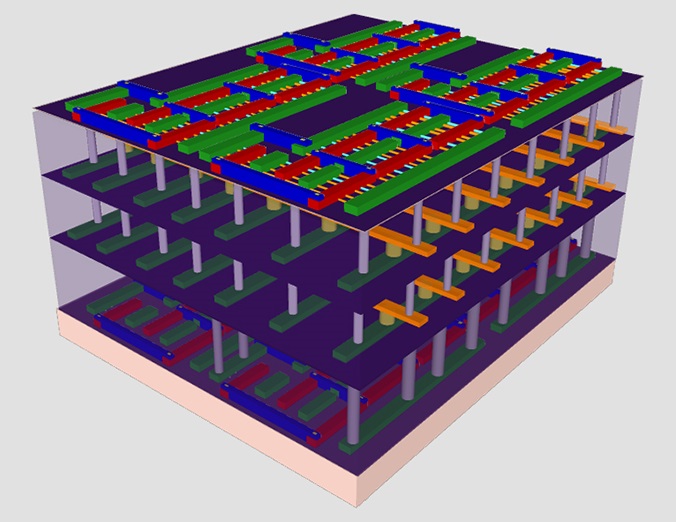
In this representation of a four-layer prototype high-rise chip created by Stanford engineers, the bottom and top layers are logic transistors. Sandwiched between those layers are two layers of memory. The vertical tubes connecting logic and memory are the nanoscale electronic “elevators.” (Courtesy of Max Shulaker)
The researchers' innovation leverages three breakthroughs. The first is the use of carbon-nanotube transistors (CNTs) to cut leakage and power drain. They started by growing CNTs in the standard way, on round quartz wafers. Then they added what amounts to a metal film that acts like adhesive tape; it lets them lift an entire array of CNTs off the quartz growth medium and place it on a silicon wafer.
The second breakthrough is a new type of computer memory called resistive random-access memory (RRAM), in which the cells of a metal/oxide/metal (titanium nitride/hafnium oxide/platinum) sandwich store data by changing from a resistive to a conductive state. RRAM not only uses less energy than conventional RAM, but it can be made at much lower temperatures than silicon memory.
Ultimately, everything hinges on the low-heat process for making RRAM, which allows it to be fabricated atop the CNT layer. While making each memory layer, the researchers were able to create thousands of vias into the logic layer below. This multiplicity of connections, or “elevators,” is what enables the high-rise chip to avoid the traffic jams on conventional circuit cards. For more information, contact Subhasish Mitra, subh@stanford.edu, or H. S. Philip Wong, hspwong@stanford.edu.
Advertisement
Learn more about Stanford University


