Optimize write speed and endurance by protecting cache memory with ultracaps
BY PIERRE MARS
CAP-XX, Sydney, Australia
http://www.cap-xx.com
Compared with hard-disk drives (HDDs), solid-state drives (SSDs) are more robust against shock, consume less power, use capacity more efficiently, and offer longer life, faster access times, and better read performance. However, SSDs face performance challenges in write speed due to some technical characteristics of NAND flash memory. But the write performance of NAND flash SSDs can be enhanced using protected cache memory — in particular SDRAM — with backup power supplied by a supercapacitor.
NAND flash endurance
HDDs have no limit to the number of erase/write cycles that can be performed on any memory location. NAND flash SSDs, however, can only be erased and written a finite number of times. This is known as the “endurance” of the flash memory, and is typically 100,000 erase/write cycles for single-level cell (SLC) NAND flash.
This endurance limit means that write operations must be spread evenly across the NAND flash blocks to prevent part of the memory from aging prematurely. This “wear-leveling” process is managed by an SSD controller, which ensures that (a) files are written to least-used memory blocks (dynamic wear leveling), and (b) static data does not remain in underutilized locations (static wear leveling).
These operations generate significant amounts of metadata, including block erase counts, translation tables, physical/logical address maps, bad block management, and error correction information, which may need to be updated and saved several times during every file operation. This metadata must be protected from accidental loss or corruption if the power supply is interrupted.
NAND flash write speed
The read/write performance of a conventional HDD is limited by the need to spin up the disk and move the head across the platter. This rotational latency and extended seek time impact the HDD’s read and write speed, most significantly during random read/writes involving small files, and less so during sequential read/writes such as recording a video, playing music, or running a virus scan.
Conversely, NAND flash SSDs don’t suffer any access latency, but their I/O performance is limited by the IC’s serial architecture:
The flash IC is organized in pages and blocks.Read and write operations can be performed on a single page.Each memory location must be erased before it can be written.Erase operations can only be performed on an entire block.A block erase takes ~2 ms typ.Writing a page takes 300 µs typ.Reading a random page takes 25 µs max.Reading sequential pages takes 30 ns min
Because an individual NAND flash IC potentially has to support a block read, a write of existing data to other pages, a block erase, and finally, another page write, even if only 1 byte is changed, the IC’s sequential write speed is slow compared to an HDD.
Fortunately, SSD performance need not be limited to an individual NAND flash IC’s performance. A typical, multichannel SSD with flash bus controllers linked to parallel banks of NAND flash ICs can use the SSD controller to interleave operations between the banks of NAND flash memory, enabling simultaneous read, erase, and write operations on multiple pages and blocks across all channels for increased performance.
Improving SSD write
Despite improvements by multichannel controllers, the erase/write limitations of NAND flash make it difficult for an SSD writing data directly to the flash ICs to match the write speeds of an HDD. Table 1 compares the overall I/O operations/s (IOPS) of a SanDisk SATA 500 SSD and a Seagate SAS HDD. Even a small proportion of random writes severely impacts the overall I/O performance of a flash SSD.
| Table 1. Effect of random writes on overall I/O performance | ||
| % Writes | Total IOPS | Sandisk SATA 500 SSD vs Seagate ST936751SS HDD |
| 0 | 5,400 | 20x better |
| 5 | 252 | 1.25x better, 1.5x worse |
| 10 | 130 | 1.5x worse |
| 20 | 65 | 3x worse |
| 50 | 26 | 8x worse |
| 100 | 13 | 16x worse |
This sensitivity to file writes reduces the advantage of SSDs in large server applications such as online transaction processing, database applications and others which involve many small updates. To resolve this, recent SSD designs incorporate a high-speed SDRAM cache, providing a read/write buffer on the data bus and a suitable location to store rapidly changing metadata generated by the controller. The cache effectively decouples SSD performance from the erase/write speed of the NAND flash memory and dramatically improves write performance.
Solutions for cache memory
Ideally, cache memory should be nonvolatile, so that if the SSD loses power, cache contents are kept and the disk is not corrupted. Currently, nonvolatile RAM solutions such as nVSRAM, FRAM, and MRAM are in their infancy and are very expensive (in excess of $50/Mbyte).
The most cost-effective solution for a protected cache today is SDRAM, with on-board power backup. There are two alternatives for providing this backup power, shown in Table 2 .
| Table 2. SSD backup power options | ||
| Power Solution | Pros | Cons |
| Secondary Battery | High energy | – Limited life (~500 cycles) – Large size (in order to provide required current) – Limited temperature range |
| Supercapacitor | – Long life – Wider temperature range (30 to 70C) | – Large size (can types) – Limited cell voltage |
| CAP-XX Supercapacitor | As above, plus – Thin, flat, and small – Higher voltage/cell – Wider temperature range (40 to 85C) | |
SSD backup power supply design with supercapacitors
Referring to Fig. 1 , typically, in an SSD the NAND flash is powered at 1.8 V (or sometimes 3.3 V), the SDRAM is powered at 3.3 V, and the controller is at ~1.2 V (although sometimes this may also be at 3.3 or 1.8 V). In the following case, we have assumed that the NAND is at 1.8 V and the controller is at 1.2 V.
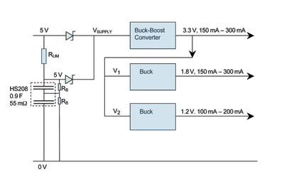
Fig. 1. A simple design for power backup in an SSD using a supercapacitor.
The load currents and duration of backup depend on the size of the SSD (and of the cache). Typically, a 5-V supply is available for the SSD.
If Rlim = 5 Ω, then the maximum initial in-rush current = 1 A and it will take 4.5 s to charge the supercapacitor to 4.75 V. A buck-boost generates the 3.3-V rail so that the supercapacitor can more completely discharge.
This will support the SSD for longer, enabling safe storage of a greater amount of cached data. A suitable buck-boost is the TPS63001, which can operate with an input voltage down to 1.8 V. Buck regulators are preferred for the 1.8- and 1.2-V supplies for maximum efficiency. The AAT2785 is a triple buck converter that would be suitable. In this case, the minimum supercapacitor voltage to support the system would be 3.3 V.
Assuming 85% efficiency for the switching regulators, the maximum load power seen by the source would be:
3.3 V x 300 mA / 85% + 1.8 V x 300 mA / (85% x 85%) + 1.2 V x 200 mA / (85% x 85%) = 2.25 W.
If LDOs are used for the 1.8-V and 1.2-V supplies, then the load seen by the supercapacitor increases to 3.3 V x 800 mA / 85% = 3.1 W, or an increase of 38%. ■
Advertisement
Learn more about CAP-XX


