Team proves new way to produce silicon wires
A simple, inexpensive method enables the production of solar cells, batteries, and sensors
Researchers at MIT and Penn State have announced a simple, inexpensive way to produce silicon wires in quantity in a highly controlled way that could be scaled up to an industrial-scale process promising to enable novel sensor, battery, and solar-cell applications. For example, silicon microwires can be used for the production of solar cells that can harvest much more sunlight for a given amount of material than a traditional solar cell made from a thin wafer of silicon crystal.
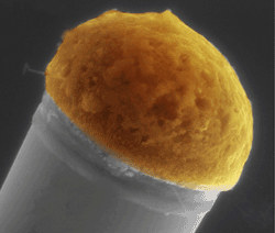
Molten droplets of copper, at top, dissolve silicon out of the surrounding silicon tetrachloride gas, in which the silicon precipitates out at the bottom of the drop and silicon microwires begin to grow. This microscope image has color added for clarity. (Image courtesy of Tonio Buanassisi at MIT.)
However, there are other methods used today for making such wires in which solar-cell prototypes have be made by several researchers. But, according to Tonio Buonassisi, mechanical engineering professor at MIT, “these methods have serious limitations.” Most require several extra manufacturing steps, provide little control over the exact sizes and spacing of the wires, and only work on flat surfaces. By contrast, the new process is simple, yet allows precise control over the wire dimensions and spacing, and could theoretically be done on any kind of curved, 3-D surface.
The researchers found that by heating and intentionally contaminating the surface of a silicon wafer with copper, the copper diffuses into the silicon. When the silicon cools down, the metal diffuses out, forming droplets on the surface. Then, it gets placed in an atmosphere of silicon tetrachloride gas, in which the silicon microwires begin to grow outward wherever there is a copper droplet on the surface.
The silicon in the gas dissolves into these molten droplets and then begins to precipitate out at the bottom of the drop to gradually build up as silicon microwire. This build up gradually elongates to form microwires each at about 10 to 20 micrometers across, growing up from the surface. “The whole process can be carried out repeatedly on an industrial manufacturing scale, or even could potentially be adapted to a continuous process,” Buonassisi said.
Space between wires is controlled by textures created on the surface, and the size of the wires is controlled by the temperatures used for the diffusion stage of the process, unlike other methods today that allow the size and spacing of the wires to be controlled independently of each other. According to Buonassisi, “The work done so far is just a proof of principle, and more work remains to be done to find the best combinations of temperature profiles, copper concentrations and surface patterning for various applications, since the process allows for orders-of-magnitude differences in the size of the wires.”
Christina Nickolas
Advertisement
Learn more about Electronic Products MagazineMIT


