Testing passive devices for thermals and noise effects
Manufacturers and users of passive components in low-V apps must pay more attention to, and learn to test for, low-level errors
BY JAMES NIEMANN
Staff Engineer, Keithley Instruments
www.keithley.com
The use of passive devices in low-voltage applications is becoming increasingly common. For example, laptops and cell phones require batteries with ultra low internal (ionic) resistance. So manufacturers and users of passive components must now pay greater attention to the materials and processes used to build them, as well as new rules about using them in low-voltage applications, in order to prevent problems previously unseen.
Thermoelectric EMFs are most common in passive components constructed of dissimilar materials, such as resistors. Design and manufacturing activities, such as testing batteries with ionic resistance, demand greater focus on the impact of noise and thermoelectric EMFs on measurement accuracy. This can be particularly challenging because very low test currents are required to measure these single-milliohm resistances.
Understanding the challenges of using passive components in low-voltage circuits, the sources of error, and proper means for characterizing them is crucial to the proper design of low-voltage devices. The test for susceptibility described here can help engineers identify which passive devices are most suitable for such applications.
Mechanics of noise
Though often lumped together, the mechanisms of thermal noise, low-frequency noise, and thermoelectric EMFs (or thermals) aren’t identical.
Thermal or Johnson noise develops when the trajectories of conduction electrons in a material are altered by the thermal vibrations of its molecules. These scattered electrons develop noise voltages when they travel through the resistance of their pathway. The spectral content of this noise is white, dependant only on the material’s temperature and resistance. All components with non-zero resistance and non-zero temperature produce some level of thermal noise.
Depending on the material or device involved, at lower frequencies, additional 1/f noise terms may begin to emerge from within the white noise floor. This kind of noise is frequently the result of material defects that behave as an electron (or hole) trap. These noise sources have the annoying property of increasing in magnitude as the bandwidth decreases, so digital filters (which increase signal observation time) aren’t helpful.
Mechanics of thermals
Thermoelectric EMFs develop wherever dissimilar materials come together in the presence of a temperature gradient. Three different effects play a role: the Seebeck, Thomson, and Peltier effects.
Seebeck effect produces a voltage that is observed when a uniformly conductive material experiences an end-to-end temperature gradient. The voltage is present whether the circuit is closed (non-zero current) or open (zero current). In practice, this voltage is difficult to measure in a single conductor, but when different kinds of conductors or materials (each with a different Seebeck coefficient) are paired to form a thermocouple, it’s much simpler to measure the difference.
When the Seebeck effect is observed within a uniformly conductive material, if the circuit is closed and a current is allowed to flow, the Thomson effect can also be observed. The Thomson effect describes how these charge carriers absorb or release heat as they pass through a temperature gradient.
The Peltier effect occurs at the junction of two dissimilar materials. Charge carriers (current) must be flowing to observe a temperature difference generated by the current passing between the dissimilar materials. Although the Peltier effect doesn’t generate a voltage, the resulting temperature changes can affect the Thomson and Seebeck voltages.
Measurement impacts
Dissimilar materials, currents, and temperature gradients are all characteristics or consequences of using passive components, so these EMFs can have a significant impact on measurement accuracy. The measurement bandwidth determines the magnitude of the inaccuracies each contributes when passives are used in real applications.
Generally, the total signal observation time determines the low-frequency bandwidth limit; the width (aperture) of the A/D conversion’s integration period determines the high-frequency bandwidth limit. With thermoelectric EMFs, these offsets persist even at dc, as long as there’s a dc temperature gradient created by a point heat source, either within the passive component or somewhere on the circuit board.
However, for passives, a change in power dissipated within or around the passive causes a temporary gradient, which equalizes according to the thermal time constants of the component as situated on the printed circuit board (PCB). In other words, the EMF can be time dependent, diminishing to near zero when temperatures are in equilibrium.
The selection process for resistors usually revolves around cost and such application requirements as temperature coefficient, voltage ratings, voltage coefficient, power requirements, and physical size. The resistor’s noise and thermoelectric properties are rarely considered.
Applications across the board have been affected by the rapid regression of supply voltage across all semiconductor industries from microprocessors to high-performance analog. Lower supply voltages require less silicon (and less cost) and can be assembled into smaller packages. However, lower volatges also mean that noise will be more significant on a percentage basis. If power/currents are lowered in concert with voltage, the same can be said for noise currents. Fortunately, smaller components can usually be PCB-mounted in such a way that minimizes thermal time constants, leading to a desirable thermoelectric footprint.
Testing
Precision and low-voltage applications like battery testing sometimes require characterizing passive components (in addition to their PCB connections). This can be tricky because the magnitude of all three thermoelectric EMF contributors depends on the temperature gradients of the connecting wires and within the components.
This last term is often overlooked. If the passive component isn’t built correctly from the correct materials, a step change in temperature of the entire component will cause temperature gradients within the component, generating an EMF. Measuring the same EMF twice can be difficult due to their dependence upon the temperature gradient and the rate of change of this gradient.
Many passive components are manufactured using different kinds of materials needed to elicit other desirable properties (for example, low temperature coefficient of resistance or a stable capacitance with applied voltage), so it’s impossible to avoid generating thermoelectric voltages within them completely. However, avoiding the unwanted temperature gradient(s) also required to generate thermoelectric EMFs is possible. A passive component’s design and application can affect the magnitude and time duration of the EMF. If components are built symmetrically, and the application is both symmetrical and isothermal (or at least if the temperature gradients are symmetrical), then the EMFs generated in each lead can match and cancel each other.
The following procedure may prove helpful in demystifying elusive thermoelectric EMFs. The most repeatable way to test a component’s thermoelectric suitability is to expose it to a temperature change at a rate equal to or higher than its normal application environment.

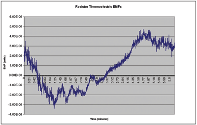
Fig. 1: The negative pulse in the above graph illustrates the resulting thermoelectric EMF generated. A temperature step back to 24C at point 1300 (at approximately 3.94 min.) causes the thermals exhibited after that point.
Figure 1 illustrates the results of such a test. In this example, a 1-kΩ film resistor was tested using a baseline voltage of 2.0 µV at 24°C. After the resistor underwent a temperature step from 24°C to 50°C, the voltage across it was measured. The magnitude of the EMF indicates how dissimilar the materials used to build the component are while the time constant (how quickly the EMF recovers) describes how quickly heat dissipates throughout the device. The dc residual (if any) results from a point source of power dissipated either within the component or from the surrounding environment.
This test is also useful for measuring the component’s response to power dissipated within it by replacing the ambient temperature shock with an internally generated power source.

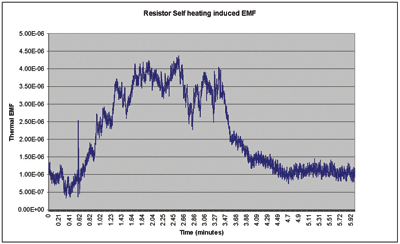
Fig. 2: To test for self-heating effects, a power step is applied to one resistor in a two-resistor 2.5-kΩ network at constant ambient temperature, and the thermoelectric voltage on the other resistor in the network, seen above, is observed. When the power step is removed (between 3.27 and 3.47 min.) , the thermoelectric EMF returns to the previous level.
The result of demonstration of thermoelectric EMF vs. self-heating for a 2.5 kΩ resistor network is seen in Figure 2. The test begins with 1.0 µV across the network. At constant ambient temperature, a power step of 160 mW is applied to one resistor in the network, and the thermoelectric voltage on the second resistor in the network is observed. Obviously, performing this type of testing requires a sensitive digital voltmeter (e.g., a Keithley’s Model 2182A Nanovoltmeter) to ensure sufficient measurement accuracy and resolution.
This procedure is useful for characterizing a passive component’s thermoelectric EMF performance in a 0°C to 50°C environment. The DUT is exposed to a thermal shock similar to the conditions it would experience in actual use.
1. Mount the passive(s) under test as it will be mounted in its intended application.
2. Using only copper connections, wire each lead of the passive component to a nanovoltmeter.
3. Place the passive(s) in an environmental chamber at 0°C and allow the system to stabilize.
4. As quickly and repeatably as possible, shock the device by raising the temperature to 50°C while measuring the voltage across it with the nanovoltmeter. Allow the device to stabilize at 50°C.
5. As quickly and repeatably as possible, shock the device again by lowering the temperature to 0°C while measuring the voltage across it with the nanovoltmeter. Once again, allow the device to stabilize at 0°C.
The resulting plot of voltage vs. time provides a good indication of the device’s thermoelectric performance. The difference between the thermoelectric voltages at each temperature should be zero in the absence of device and interconnect temperature gradients.
If residual thermoelectric voltages are present, then either the component under test has not yet reached thermal equilibrium or there are gradients within the environmental chamber. During the transition between temperatures, device construction symmetries, materials, and thermal resistances will define the peak thermoelectric EMF as well as the recovery time. As in Figure 2, power dissipated within a component can fuel the thermal gradients that cause the thermoelectric EMFs. ■
Advertisement
Learn more about Keithley Instruments


