These switches expand camera design possibilities
BY ENRIQUE O. RODRIGUEZ
Fairchild Semiconductor
South Portland, ME
http;//www.fairchildsemi.com
As countries expand their 3G capabilities, customers are adopting new communication media including video conferencing. This requires smartphone devices that have two peripheral cameras: a low-resolution camera (typically VGA) for video conferencing and a high-resolution camera (over 3 Mpixels) for picture taking.
On the engineering side of the mobile handset this can present a design challenge because typically the video camera and high-resolution camera share the same baseband processor interface. As the main camera increases in resolution it also increases in speed, which means parasitic components of the connected VGA camera interface now become a bigger factor.
The designer either has to limit the amount of parasitic components of the VGA transmission “stub” or isolate the interface to maintain signal integrity. A growing trend is to implement an isolation analog switch in this path to isolate the transmission line “stub” and maintain signal integrity.

A 3G smartphone typically is a bar-style phone with a large (HVGA or higher) LCD screen and two cameras. Its design has been created in order to focus the customer to the software applications. Although video conferencing via mobile devices is a fairly new concept in a number of countries, the limitation to this point has been the bandwidth of the network.
Once bandwidth is not of a concern, then applications such as video conferencing start to become common place. Phone markets in several countries are experiencing growth in demand and the use of video conferencing.
To date, most video-conferencing smartphones have been designed with a VGA camera for video conferencing and 1.3 to 3-Mpixel camera for picture-taking. The VGA camera module is a 640 x 480 sensor running at 30 fps with a reference clock of approximately 30 MHz (depending on the camera module design) and 8 to 10 bits of data. The 3-Mpixel camera is a 2,048 x 1,536 sensor running above 30 fps with a reference clock of greater than 48 to 100 MHz (depending on the camera module design) and 8 to 12 bits of data.
The signal paths of both cameras (including clock, data, and command lines) share the baseband processor interface to reduce both PCB layout and processor complexity. The camera interface is routed from the baseband processor to the camera modules through the PCB, connectors, and flexes.
At some point of the flex there will be a split between the routing of the VGA camera and the higher-megapixel camera. Selecting the active camera module is done by enabling separate clock lines for each. This layout requires two clock lines in the typical implementation.
Limitations
This design has a number of limitations, including placement of camera modules, resolution of cameras, and interference with RF bands. The mechanical design typically dictates where the modules are located.
The limitation of the placement depends on the differential impedance of the flex cable as well as all the parasitic components associated with that section of the flex. It is these parasitic components that will “limit” the performance of the alternate data path.
For example, if a designer wanted to use a 3-Mpixel camera for video conferencing and an 8-Mpixel camera for the main camera, the transmission line “stub” of the 3-Mpixel camera in parallel with the main camera would create signal reflections and unacceptably poor signal integrity. This poor signal integrity will generate radiated EMI and limit the performance of the 8-Mpixel camera module.
In addition to signal integrity problems, the secondary camera path, when not in use, will still be driven from the processor. This will mean that it will act as an antenna radiating EMI on the unused path. As the clocks for the camera modules get higher in frequency, they will start to interfere with the RF bands, creating a desense problem.
Solution: Camera switch
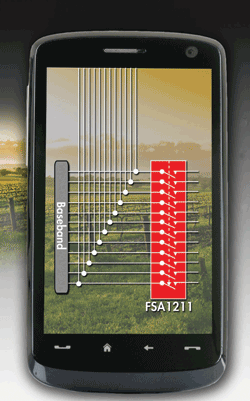
A trend in the industry is to solve these issues using a camera switch. A camera switch is an SPST analog switch that isolates the unused stub from the main parallel connection. In the camera application, this would be a 12-bit switch for the clocks, data, and control bits.
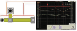
To understand how the camera switch will help to achieve higher performance, we analyzed the camera module design of a latest production smartphone. This particular smartphone has a 5-Mpixel camera and a VGA camera in a bar-style form factor. In this phone, the baseband processor-to-camera flex cable (FPCB) leads from the main board that houses the baseband processor to the VGA camera module board. The flex cable is composed of two sections: the main connector 1 and the secondary connector 2. To evaluate the characteristics of the flex cable we used time domain reflectometry (TDR) to calculate the differential impedance, which ultimately indicates the integrity of the signals.
Figure 1 shows the TDR response of the flex cable that was disconnected from the main board but still connected to the two camera modules. Reading the graph shown on the right side of Fig. 1, we can see that the differential impedance of the first section from connector 1 to connector 2 is relatively flat at approximately 75 Ω. This comes as no surprise since the flex cable shielding is uniform along its length and there are no components that would cause impedance discontinuities.
The key to this analysis is the second section of the flex from connector 2 to the camera module. As you can see in the TDR image of Figure 1 the impedance of the two camera flex stubs connected in parallel with each other drops the effective impedance seen by the signal by approximately 12% to 15%. This drop in impedance is a limitation to the maximum camera speed in this path because it will deteriorate higher-speed signals. As camera signal speeds become increasingly faster, the amount of capacitance on the line will limit the bandwidth. Additionally, reflections of signals from the un-isolated inactive camera path will further degrade signal integrity by introducing artifacts in the signal transitions. Depending on the baseband processor, length of flex and camera module, data may ultimately be corrupted due to a missed clock cycle. This will cause the image data to be incorrect. A side effect of the reflections from the un-isolated camera stub is that the signal degradation can have high-frequency EMI content which could cause a desense problem in the RF bands of communication.

Fig. 1. Smartphone example camera flex TDR with connector 2.
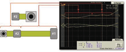
In contrast, if we detach connector 2 from the flex cable and retake the measurements, the results can be seen in Fig. 2 .

Fig. 2. Smartphone example camera flex TDR without connector 2.
As you can see, the capacitive coupling or “dip” caused by both cameras connected in parallel that was seen in Fig. 1 is gone, replaced by a rather consistent approximately 100-Ω differential impedance in that particular section. This increase in impedance is due to the isolation of the second camera from the signal path at connector 2. This creates a signal path that can now tolerate higher frequencies because of the reduction of discontinuities and the resulting improvement in signal integrity.
This is the core value of the camera switches: providing designers with the ability to isolate the inactive camera path, mimicking the detachment of connector 2, from the system. It is for this reason that camera isolation switches, such as Fairchild’s 12-port FSA1211, enable improvement in placement and resolution of camera modules in mobile devices.
These isolation switches have been designed specifically for camera applications, taking into account the higher bandwidth well above 750 MHz, its lower on-resistance and on-capacitance. But the core is the ability to isolate the system from the parasitic components. In addition to their minimized crosstalk technique, the camera isolation switches can also be placed on the flex cables due to the availability of these devices in small package form factors.
As camera modules continue to increase in resolution and camera signal speeds, more camera designers are transitioning to using camera isolation switches to enable their designs. Additional benefits of using these switches in the camera path include reduction in radiated EMI from signals on the otherwise un-isolated parallel camera path and reduction in the components needed due to this EMI.
As smartphones continue to increase in camera resolution, camera isolation switches will aid in their development. With their high-performance design, these switches cannot only solve a significant design issue, but also expand camera design possibilities. ■
Advertisement
Learn more about Fairchild Semiconductor


