Sustained processing performance is nearly equal to peak
BY MIKE STRICKLAND
Altera, San Jose, CA
http://www.altera.com
The architecture of an FPGA allows the implementation of many algorithms where the sustained performance is much closer to the device’s peak performance than when using either a quad-core CPU or a general-purpose graphics processor (GPGPU). The strong benchmarking results from FPGA accelerators continue to improve with the appropriate focus on the silicon, arithmetic, and library foundations. Since even the largest FPGAs currently consume less than 30 W, they can be used in many applications. Several trends are converging to make FPGA acceleration of algorithms more attractive. These include the following:
• FPGAs today are large enough to encompass larger algorithms. It is now possible to fit options-pricing algorithms or 1-Mpoint fast Fourier transforms into FPGAs. The latency to off load an algorithm from the CPU to an FPGA is minor compared to the time saved by the algorithmic speedup.
• Single-core CPUs have hit a power/cooling wall. The move to multicore CPUs is well underway, however existing software written for single-core must be rewritten to extract parallelism for reasonable performance scaling.
• Active support of FPGA coprocessing. In some cases, these CPU interfaces — AMD with the Torrenza Initiative and Intel by licensing FSB and QPI to FPGA vendors — support 8 Gbytes/s speed with latency for posted writes of under 140 ns.
FPGA benchmark results have shown excellent Monte Carlo floating-point results using a socket accelerator compared to dual quad-core CPUs or a GPGPU (see Table 1 ).
| Table 1. Monte Carlo Black-Scholes Performance Comparison (CPU and GPU results at 1M paths per option) | |||
| Monte Carlo | 2 Quad-Core CPUs | nVidia 8800 | XD2000i + 2 EP3S260s |
| Precision | Single | Single | Double |
| Paths per second | ~240M | ~900M | 1.8G |
| RNG type | Halton | Halton | Mersenne |
| Source | RapidMind | RapidMind | XtremeData |
How does an FPGA running at 150 to 250 MHz deliver better results than a quad-core CPU running at 2 to 3 GHz or a 128-core GPU running at 1.35 GHz? As demonstrated in the Monte Carlo Black-Scholes algorithm, the FPGA architecture has unique capabilities that combine to deliver the impressive results.
Features of FPGA architecture
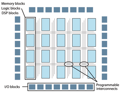
Fig. 1. FPGA architecture.
Flexible FPGAs can be programmed and reprogrammed as needed. A typical FPGA comprises an array of logic blocks, memory blocks, and DSP blocks, surrounded by programmable interconnects that can be configured with software (see Fig. 1 ). This architecture enables the following features:
• Function parallelization : replication of a function many times.
• Data parallelization : handling of data arrays or data matrices.
• Custom instruction with pipelining : streaming data with one result per clock.
• Huge primary cache bandwidth and size : 3X to 10X compared to GPGPUs.
• Flexible routing of datapath : huge crossbar routing transfers data in one clock.
• Concatenation of functions and data flow : all in one clock.
• Custom off-chip I/Os : protocol, bandwidth, and latency as needed.
• Scalable roadmap : larger arrays have plenty of headroom for power and cooling.
The advantages for parallelization and pipelining are pretty obvious, but FPGAs also have an advantage in primary cache and bandwidth over GPGPUs. Within the FPGA, logic is surrounded by memory blocks. The XDI module has a 3.3-Mbyte primary cache with a bandwidth of 3.8 Tbytes/s about 5 to 10 times larger than the primary cache (for streaming processors) on the nVidia 8800 GTX GPGPU.
The advantage also includes the FPGA’s ability to use the excess routing bandwidth to construct the data path and memory access flexibly and directly to each logic block. The programmable interconnects shown in Fig. 1 provide a large amount of routing bandwidth. Modules and boards can be designed as needed for off-FPGA bandwidth, memory size, and latency, and I/Os can also be customized.
A final aspect of FPGA architecture is the ability to scale to larger arrays of logic, memory blocks, and DSP blocks. Logic and primary cache sizes scale together. With the largest FPGAs currently consuming about 30 W peak, the FPGA architecture has plenty of room to scale to new process geometries without hitting current datacenter power and cooling limits.
While FPGA architecture has numerous outstanding capabilities, several areas must come together for a superior CPU coprocessing solution.
Silicon and arithmetic foundations
Most algorithms using double-precision floating point have about a one-to-one ratio of addition and multiplication operators. In an FPGA, the addition core uses logic, the multiplication core uses the DSP blocks, so the FPGA must have a balanced ratio of logic to DSP blocks. Another FPGA feature is Programmable Power Technology, which allows each logic block, DSP block, and memory block to be programmed to run in higher- or lower-power mode depending on the design timing requirements.
Floating-point operator cores have been improved to run at higher clock speeds and to use fewer DSP blocks and less logic. Using a floating-point compiler, the logic to route 64-bit data paths between different floating-point operator cores can be reduced.
Combining the steps of normalizing (converting fixed to floating-point format) at the end of one floating-point operation and then denormalizing (converting floating-point to fixed format) for the input of the next floating-point operation can be significantly reduced. The entire datapath for a mathematical expression with floating-point operations can be fused together, saving up to 40% in logic and increasing clock speed slightly.
The right mix of floating-point operators is important. If an algorithm has many transcendentals (exponents, logs, etc.), the FPGA can be configured with as many as are needed. In GPGPU designs, a few hard blocks are added for such functions, but at a much smaller ratio than single-precision floating-point logic. Function libraries are needed to employ algorithmic tricks, abstract the hardware details, and optimize for particular FPGA resources.
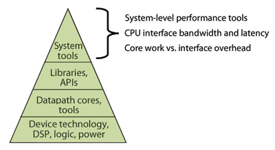
Fig. 2. A foundation for FPGA acceleration with a system-level solution.
Building on the silicon, arithmetic, and library foundations, the system-level solution in Fig. 2 takes care of the tool chain, module/board design, CPU interface, and data passing from the CPU to the FPGA-based accelerator by using the expertise of partner companies.
Enabling sustained performance close to peak
For tasks that can be parallelized or pipelined, FPGA capabilities frequently enable a much higher sustained performance relative to peak performance and keep all device resources available. Starting with an example of the Monte Carlo Black-Scholes benchmark, an equation pipeline was created to run at 150 MHz.
| Table 2. Peak floating point performance of four solutions using the Black-Scholes benchmark | ||||
| 1:1 Adder/Multiplier | 2 Quad-Core CPUs | nVidia 8800 | XD2000i w/1 EP3S260 | XD2000i w/1 EP3S260 |
| Precision | Single | Single | Single | Double |
| Clock (MHz) | 2500 | 1350 | 280 | 256 |
| FP ops/cycle | 8 | 2 | 1 | 1 |
| # of Cores | 8 | 128 | 384 | 192 |
| Peak GFLOPS | 160 | 346 | 108 | 49 |
On each clock, random numbers generated on the FPGA by a Mersenne Twister core were fed (concatenated) into this “custom instruction” with one result per clock. Twelve of these custom instruction pipelines fit in the two FPGAs on the module, yielding 12 × 150 M = 1.8 G results/s with double-precision floating-point logic. With additional tuning, twice this performance is expected.
It is interesting to compare sustained vs. peak-performance floating-point capabilities of different architectures. Table 2 shows the peak performance for single-precision floating point for four possible solutions. Since the Black-Scholes equation requires more functions (exponent, square root, etc.) than the usual addition and multiplication functions, the total GFLOPS in the Black-Scholes results are not counted.
| Table 3. Monte Carlo Black-Scholes performance/power ratio | |||
| Monte Carlo | 2 Quad-Core CPUs | CPU + nVidia 8800 | CPU + XD2000i w/2 EP3S260s |
| Precision | Single | Single | Double |
| M results per second | 240 | 900 | 1800 |
| Performance/peak GFLOPS | 1.5 | 2.6 | 12.0 |
| Power | ~150W | ~215W | ~110W |
| Performance/watt | 1.6 | 4.2 | 16.4 |
| Results/clock | 0.1 | 0.7 | 6.4 |
Table 3 shows the ratio of Black-Scholes results to peak GFLOPS to get a relative measure of sustained performance vs. peak performance. The FPGA has the best sustained performance compared to peak performance. Also, the FPGA has the best raw performance in double-precision logic compared to single-precision logic for the other two accelerators, as well as the best performance/watt.
For many algorithms that contain parallelism or that can be pipelined, the sustained performance of FPGAs can approach peak performance due to excess routing bandwidth that enables a custom datapath, letting logic access memory or results from another logic block in one clock. While fixed architectures have a predetermined set of logic blocks for different functions, the FPGA can be configured to have the optimum ratio of logic functions for a given algorithm for the best use of device resources. ■
Advertisement
Learn more about Altera


