What is “the forgotten NAND”? In the overall scheme of NAND memory, low-density SLC NAND may have a small market share, but it plays an important role. While everyone is talking about high density flash and 3D NAND, low-density SLC is busy playing an important role in things we touch every day.
Electronic Products ' Jim Harrison explores some frequently asked questions regarding low-density SLC NAND – and the role it plays in our everyday lives.
Q WHAT IS LOW-DENSITY SLC NAND?
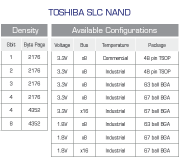
A Invented by Toshiba, SLC (Single Level Cell) NAND is the original NAND architecture. Its much higher endurance (vs.MLC) makes it ideally suited for a variety of consumer and industrial applications where longevity of supply is important. Low-density SLC refers to (While many applications are moving to MLC, SLC is still around in a big way — even if it does fly under the radar when compared to the attention its MLC NAND counterparts receive. SLC is the only memory currently available which can provide high levels of endurance, long life cycles, high reliability and wide temperature ranges. Low-density SLC NAND is available in an asynchronous (or legacy) interface only, with an interface speed of up to 50 Mbytes/s. By way of comparison, high-density SLC and MLC NAND devices typically have the toggle-mode DDR interface, which supports an interface speed of up to 400 Mbytes. Available packages for low-density SLC NAND include TSOP and BGA. The BGA is available in a new, smaller 67-ball version — as well as the older 63-ball version. The most popular configurations are 3.3-V, x8 TSOPs and 1.8-V, x8 BGAs.

Q WHERE CAN LOW-DENSITY SLC NAND BE FOUND?
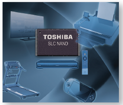
A SLC has a relatively small market share in terms of total NAND bits, but it runs a lot of things that people take for granted — it has a substantial impact. It is found in a lot of places that people don’t necessarily know about, including TVs, ink-jet printers, digital cameras, set-top boxes, toys, exercise equipment, automation control, printers, teleconferencing equipment, POS terminals, and more. Parts with –40° to 85°C temperature range are especially popular for industrial and outdoor applications.
Q WHAT FUNCTION DOES LOW-DENSITY SLC NAND PERFORM IN THESE PRODUCTS?
A It’s the ROM (read-only memory) for a lot of these products — used for boot up and small amounts of datalogging. People tend to take it for granted when they press a button on their printer and it boots up right away. SLC NAND makes it happen.

Q WHAT DOES THE FUTURE HOLD FOR LOW-DENSITY SLC NAND?
A It will be around for quite some time, as there aren’t any good alternatives available at the moment. NOR flash is more suited to code-storage applications, and, for any given lithography process, the density of the NAND flash will always be higher than NOR flash which makes NAND a lower price per gigabyte option. For example, the highest-density NOR commercially available is 1 Gbit, while SLC NAND starts at 1 Gbit and goes up from there. In regard to MLC, although it offers high density and low cost per bit, it can’t compete when it comes to endurance, temperature range, and speed. Additionally, MLC NAND is not available in these low densities anymore.
Q WHAT OTHER TYPES OF SLC NAND ARE AVAILABLE?
A SLC NAND is available for industrial temperature operation, and in both x8 and x16 bus widths.
Q WHAT DOES THE FUTURE HOLD FOR SLC NAND?
A ECC requirements for SLC NAND have increased from 1 bit/512 bytes to 8 bits/512 bytes. Therefore, it is expected that SLC NAND flash with built-in error correction (ECC) hardware will become more popular. Toshiba offers the BENAND™ (1-bit ECC NAND) family to meet this need. BENAND™ is SLC NAND with embedded ECC, which removes the burden of ECC from the host processor. Currently, the lowest density SLC NAND available is 512 Mbits. In the near future, the lowest density available will be 1 Gbit. With enough ECC, SLC NAND can still reach 100,000 write/erase cycles, but, with the minimum recommended ECC, reaching 60,000 write/erase cycles is more common.
Q WHAT DOES TOSHIBA OFFER IN THE WAY OF SLC?
A I recently talked with Brian Kumagai, director of NAND Flash Memory Products for Toshiba America Electronic Components, to find out more about what they are doing in this area. Toshiba has the full range of SLC NAND available- including the aforementioned BENAND family. According to Kumagai, “Toshiba developed NAND-type flash technology in 1984 and was the world leader in promoting its practical use. We continue to maintain our leadership position in high density, advanced processes, and mass-production technology. SLC chips can read and write large amounts of data at high speed, support high-write/erasecycle endurance, and offer excellent reliability. Toshiba has developed SLC devices to meet the diverse needs of different embedded applications. Our lineup for SLC NAND ranges from mid-capacity models (those with a capacity of between 1 and 4 Gbits) to large capacity models (those with a capacity of 8 Gbits or more). For these SLC NAND products, we provide support related to driver software, and technical assistance for developing NAND flash products.”
Advertisement
Learn more about Toshiba


