Higher integration, multiple power domains, and more analog lead to more functional issues
BY GREG HACKNEY
Mentor Graphics, Wilsonville, OR
www.mentor.com
The future of IC design verification does not lie in doing more of the same in less time. The increasing complexity of IC design requires a completely new way of thinking about IC design verification.
The complexity of DRC rules increases with shrinking geometries. It is not that the laws of physics change with shrinking IC feature size; they are just more strictly enforced. At one time, there was only one minimum space requirement per layer. As the minimum space shrunk, lithography and manufacturing issues required a more complicated set of rules. The minimum space became dependent on the width of objects on the layer.
The first specialized verification solution was a table-driven DRC tool with rules that specified the minimum space for a range of widths. Later verification tools moved to equation-based checks; this allowed the minimum space requirement to be varied continuously with the width of the adjacent objects. The next stage will have to be verification tools that specify minimum widths and spacing that are dependent on, and specific to, the type of circuitry involved in a design.
Next-generation integrated circuits are characterized by higher integration, increasing use of multiple power domains, inclusion of more analog and other exotic types of circuitry, and increased I/O components. All of these trends lead to more functional issues, more rules to prevent the issues, and more need to verify the rules.
Multiple power domains
Multiple voltage domains imply that some signals will cross from one domain to another. Such signals require special checks such as for passing through level-shifter circuits. Special protection might be required where the ground nets of the two domains connect. Higher-voltage signals might require different width and spacing rules.
All of these scenarios require a verification tool that can automatically identify a circuit’s or signal’s power domain and then verify special rules. The check for level-shifter circuits requires the ability to identify signals that originate in one power domain and terminate in another and the ability to identify level-shifters.
Analog circuit needs
Analog circuits have a number of special requirements. A simple example is matched devices. Analog circuits rely on matched devices having the same electrical characteristics within a very tight tolerance. This requires a lot more than matching transistor widths and lengths. To minimize manufacturing variances, matching devices must be laid out close together. The devices must also be placed symmetrically and in a similar local environment to avoid imbalanced lithographic distortions and directional manufacturing process differences.
Proximity and symmetry can be checked with a traditional DRC tool, but how can we recognize which devices to apply the checks to? Marker layers have been one way that designers identified circuitry that required special rules, but they have several deficiencies.
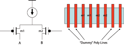
First they can be misapplied. An analog device without an analog marking layer will not be properly checked. It is very easy to mistakenly place maker layers over circuitry that should not have them. Second, marker layers do not have enough information to allow sophisticated checks: they indicate only that a particular device must be matched to some other device, but not to which one (see Fig. 1 ).

Fig. 1. Schematic for a matched pair of MOS devices and a partial layout that can be used to demonstrate the rules for diffusion (blue) and poly (red) layout.
What is needed in this kind of situation is a verification tool (such as Calibre PERC — programmable electrical rule checker) that automatically recognizes analog circuits, either from the schematic or from the layout (or both), identifies specific devices, and applies special or customized DRC rules.
Issues with ESD protection
The number of I/O cells was once limited by the number of bonding pads that could be placed around the perimeter of a die. In that environment, the size of the I/O circuitry was not critical. In particular input circuitry, unlike outputs, did not require large driver transistors and could be made small, with plenty of space to include ESD protection.
Once the limits imposed by perimeter bonding pads were broken, the size of input circuits began to be important. As geometry sizes shrunk, so could input cell sizes. The problem is that the size requirements of the ESD protection does not shrink. In 2005, Boselli et al. predicted a reduction in the high-current capability of ESD components with technology scaling.
To prevent this from limiting the number of inputs a chip can support, the ESD protection is separated from the input circuitry and shared among inputs. But this leads to new requirements for chip-level verification. Every input must be properly connected to ESD protection, and the connection must be made in a way to ensure that the input will actually be protected (otherwise we exercise a variant of one of Murphy’s laws of circuitry — the circuitry protected by a fuse protects the fuse by blowing first).
Preventing latchup
Latchup has long been an issue in bulk CMOS integrated circuits. Latchup occurs when parasitic bipolar transistors have current injected into their emitter-base junction by an ESD event, thermal stress, or ionizing radiation.
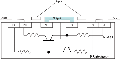
In a p-substrate process, the n+ sources and drains of the n-channel MOS transistors act as emitters of lateral npn bipolar transistors. The p-substrate acts as the base of the npn device and the n-well acts as the collector. The p-substrate also acts as the collector of a pnp device and the n-well acts as the base. The p+ sources and drains of the p-channel MOS transistors act as the emitter of the pnp device.

Fig. 2. The n-well forms the base of the pnp transistor and the p+ attached to VCC is the emitter. Current injected into the pnp emitter-base junction starts latchup.
As shown in Fig. 2 , in the presence of ionizing radiation, thermal stress, or over-voltage stress, current can be injected into the pnp emitter-base junction. Once it is forward-biased, current flows from the n-well into the p-substrate. this turns on the npn device which increases the base drive to the pnp.
Latchup prevention techniques include modification to process steps, use of special geometries to isolate input protection devices and chip outputs, and use of robust power distribution, along with enhanced termination of wells and substrates. Verification of isolation geometries and robust power distribution can only be done with a circuit-aware tool.
Additional issues
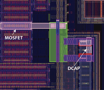
There are numerous other electrical and circuit-dependent rules that should be verified. These can broadly be characterized as methodology checks. They are often specific to one design group and based on lore that is “known to work.” One example of such a methodology is use of decoupling capacitors. The rule-of-lore is that capacitors of a certain size must be placed “close” to large MOSFETs to filter power surges (see Fig. 3 ).

Fig. 3. An example of a rule-of-lore is that capacitors of a certain size must be placed “close” to large MOSFETs to filter power surges.
Automated verification and future challenges
What do we need from IC design verification tools and solutions to address these issues? They must incorporate functions that currently exist in a variety of IC analysis and verification products. But they must also include one capability that has not been generally available—the ability to do programmable analysis of electrical circuits – to apply special checks or analysis only to specific parts of the circuit. The goal would be to avoid requiring the designer to identify the parts of the circuit with marker layers or other manual means to eliminate false positive and false errors. Identifying specific parts of the circuit automatically requires analyzing the netlist to identify subcircuits that perform specific functions such as SRAM cells, current mirrors, ESD protection structures, and device power domains.
Computer scientists will recognize that the general subcircuit recognition problem is a form of the subgraph isomorphism problem which is known to be np-complete. This means that there is no known solution that will always run in a reasonable amount of time. For practical circuits, this problem can, in general, be overcome using techniques found in layout versus schematic (LVS) comparison algorithms. Additionally, we can use the fact that many of these subcircuits contain specialized devices which can be identified by a layout circuit extraction. These specialized devices can be used as hints to speed-up finding subcircuits. The finding of specialized subcircuits must be programmable so that the person responsible for creating the specialized rule verification is able to find arbitrary subcircuits.
Besides programmable circuit analysis, what else do we need from a verification solution to address these issues? Ideally, we should be able to start with a netlist or a layout or both. This requires the functionality of a standard LVS tool (circuit extraction from layout and source versus layout netlist comparison to cross-correlate the two). Specialized layout checks require the functions of a standard DRC tool (specialized spacing checks, density checks, symmetry checks).
ESD checks may require that we know the resistance between protected devices and the protection circuitry, which means we must be able to run parasitic extraction. But we don’t need to run parasitic extraction on the entire design. To save time, we want to run resistance-only extraction on signals that participate in the ESD protection.
To verify balanced loading on analog devices, we need to be able to extract and reduce interconnect to simple RC representations. Checking that devices match in analog circuits requires specialized geometric checks. But these checks are run only on selected devices — based on connectivity. Similarly, we can envision circumstances where we may want to run specialized LVS device checks based on connectivity.
Whatever solution we use, it must provide for integration with other analysis tools. Some ESD rules are based on current density limits. Calculation of current densities is not currently done by any of the previously mentioned tools. But it is easy to imagine checks that require running simulation on a portion of the circuit. And, of course, we need a convenient way to assemble all the parts into a flow that implements specialized checks.
As much as possible, a good automated flow would hide the details of all the underlying parts. This means encapsulating the details of common operations into reusable high-level functions that make sense to whoever is specifying rule verification. The only way a verification-tool developer will be able to determine what these high-level blocks are is to implement complete solutions for a number of the problems outlined here.
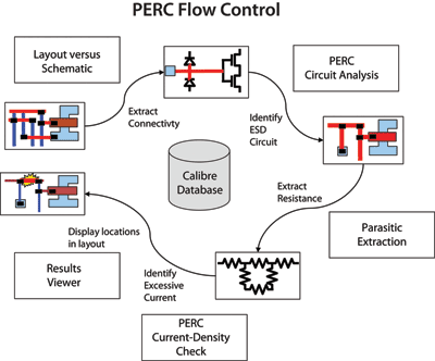
So what would such a solution look like? As said earlier, ideally it is an integrated verification system, instead of a collection of point verification tools. Let’s look at how such a system would be used for an ESD check (see Fig. 4 ).

Fig. 4. Control of the flow can be done using Calibre PERC. A PERC flow allows running LVS, circuit analysis, limited extraction (resistance only) and the ability to program entire flows. Circuit analysis can be called on just a netlist, then the layout can be loaded and special DRC checks run.
We start with a set of industry standard tools. Anyone that has seen a modern LVS deck will know that creating efficient device recognition and circuit extraction rules is time consuming. We need to be able to reuse that effort for maximum efficiency.
Next we need a way to analyze extracted or original netlists to identify subcircuits and check rules that can be verified with only a netlist. Traditional LVS tools have a very limited capability in this area, so a new solution is needed. In this example, we are looking for input circuits that need to be protected from ESD events and ESD protection structures connected to them. The lack of an ESD protection structure would be flagged as an error at this point.
For the particular check we are doing, we need to know the resistance network of the interconnect between protected devices and ESD protection structures. To do accurate current-density analysis and error reporting, we need a detailed (non-reduced) resistance network with individual resistors associated with layout polygons. This is a task for a parasitic extraction tool. Because of the specialized needs of the check (specific nets, resistance only, tied to the layout), it is best to use an integrated tool.
Finally, errors need to be presented to the designer. In this case, using the Calibre results viewing environment, violations can be highlighted in the original layout and in the source schematics using industry standard layout and schematic capture tools. A persistent, disk-resident database stores original data and the results of each step in the process. In this diagram, a programmable interface (via PERC) is used to control the overall flow (see Fig. 4).
The preceding is an example of one narrow class of checks. Other example checks might make use of DRC rules. With this flow, we also have implemented ESD checks based on point-to-point resistance, analog symmetry rule checks using DRC in the PERC flow, and latch-up checks that measure the resistance from power/ground connections through taps to MOS device source/drains.
We have only begun to scratch the surface of previously unsolved verification problems. The Calibre integrated programmable verification platform enables development of novel solutions to design verification problems that were previously unsolved or solved with expensive error-prone manual methods. ■
Advertisement
Learn more about Mentor Graphics


