The impact of clock generator performance on data converters
Selecting the right components for clock generation and data conversion enables a designer to extract the best performance from a given architecture
Hittite, Chelmsford, MA
www.hittite.com
Data converters are critical elements in communication systems forming bridges between analog transmission media such as fiber optics, microwave, RF, and digital processing blocks such as FPGAs and DSPs. System designers often focus on selecting the most appropriate data converters for the application, while much less consideration may be given to the selection of the clock generation devices supplying the data converters.
A broad range of clock generators with widely different performance attributes are available. However, without careful consideration of clock generator phase noise and jitter performance characteristics, data converter dynamic range, and linearity performance can be severely impacted. This article discusses the effect of clock generator phase noise and jitter on the dynamic range and linearity of data converters (ADCs and DACs) in detail. Theoretical analysis of clock jitter on converter SNR is presented and simulation results are provided using Hittite high-performance clock generators.
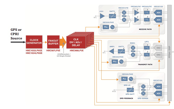
Hittite Microwave has developed a unique line of high-performance clock distribution and clock generation products that enable the system designer to maximize the performance from data converters. The HMC1032LP6GE and the HMC1034LP6GE are SMT packaged clock generators, which are ideal for a wide range of high-performance cellular/4G infrastructure, fiber optic and networking applications, and deliver best-in-class jitter and industry-leading phase noise floor. The HMC987LP5E 1-to-9 fanout buffer is ideal as a clock driver in critical applications and features an ultra-low-noise floor of 166 dBc/Hz. Key specifications for these devices are shown in Tables 1 and 2 .
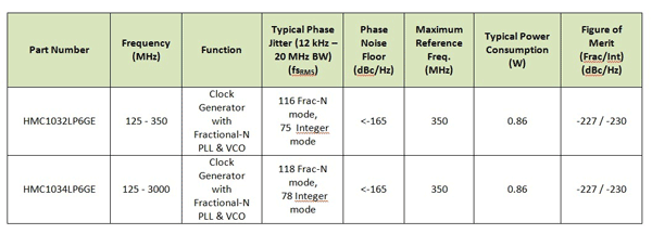
Table 1: Hittite’s clock generators: Typical performance characteristics

Table 2: Hittite’s clock distribution products: Typical performance Characteristics
System considerations
A typical LTE (Long Term Evolution) base station using MIMO (Multiple Input Multiple Output) architecture is shown in Fig. 1 . The architecture consists of multiple transmitters, receivers, and DPD (Digital Pre-Distortion) feedback paths. Various transmitter/receiver components, such as data converters (ADCs/DACs), and local oscillators (LO) require low-jitter reference clocks to improve performance. Other baseband components also require clock sources of various frequencies.

Fig. 1: Clock timing solutions for a typical LTE basestation using MIMO architecture.
The clock source used to achieve inter-base station synchronization typically comes from a GPS (global positioning system) or CPRI (common public radio interface) link. Such a source typically has excellent long-term frequency stability; however, it requires frequency translation to the required local reference frequency with excellent short-term stability, or jitter.
A high-performance clock generator such as the HMC1032LP6GE performs the frequency translation, and provides a low-jitter clock signal which may then be distributed to various base station components. Selecting the optimal clock generator is critical because a suboptimal reference clock contributes to higher LO phase noise, resulting in higher transmit/receive EVM (error vector magnitude) and system SNR (signal-to-noise-ratio). High clock jitter and noise floor also affects data converters by reducing system SNR, and introducing data converter spurious emissions, thereby further reducing the data converter SFDR (spurious free dynamic range). Consequently, a low-performance clock source ultimately reduces system capacity and throughput.
Clock generator specifications
While there are various definitions of clock jitter, the most applicable definition in data converter applications is “phase jitter,” which is specified in time domain units of picoseconds rms or femtoseconds rms. Phase jitter (PJBW) is the jitter derived by the integration of the clock signal’s phase noise over a specific range of offsets from the carrier and is given by the following equation:

fCLK is the frequency of operation; fmin/fmax indicate the bandwidth of interest, and Sϕ(fCLK) represents the SSB phase noise. The upper and lower limits of the integration bandwidth (fmin/fmax) are unique to each application and are set by the relevant spectral content that the design will be sensitive to.
A designer’s goal then is to choose a clock generator with the lowest integrated noise, or “phase jitter” in the desired bandwidth. Traditionally, clock generators are characterized by integrating over 12 kHz to 20 MHz, which is the specified requirement for optical communication interfaces, such as SONET. While this may be applicable in some data converter applications, a broader spectrum of integration, particularly extending beyond 20 MHz is usually needed to capture the relevant noise profile of the sample clock for a high-speed data converter.
When measuring phase noise, the noise at offsets far from the carrier frequency, i.e. the actual clock frequency used for data converter sampling, are commonly referred to as “far-from-carrier” phase noise. The limit of this noise is usually referred to as the “phase noise floor,” as shown in Fig. 2 . This figure shows the actual measurement plot of Hittite’s HMC1032LP6GE clock generator. The phase noise floor takes on additional importance in data converter applications because of the sensitivity of the converter SNR to broadband noise on its clock input. When designers evaluate options for clock generators, the phase noise floor performance must be considered as a key benchmark.
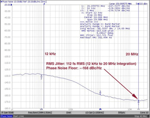
Fig. 2: Phase noise and jitter performance of HMC1032LP6GE.
Figure 2 indicates an integrated phase jitter of ~112 fsRMS in the 12-kHz to 20-MHz integration bandwidth, and a phase noise floor of ~168 dBc/Hz when operating at ~160 MHz. It is worthwhile to note here that when considering the most appropriate clock generator for a data converter, a designer should refer not only to the phase noise measurements in the frequency domain, but also to clock signal quality measurements such as duty cycle and rise/fall time in the time domain.
Data converter performance
In order to describe the performance impact of clock noise on data converters, a converter can be thought of as a digital mixer, with a subtle difference. In a mixer the phase noise of the LO is added to the signal being mixed. In a data converter the phase noise of the clock is imposed on the translated output, but is suppressed by the ratio of the signal to the clock frequency. The clock jitter causes errors in the the sampling time, which manifest themselves as reduced SNR.
The time jitter, Tjitter, is simply the rms error in the sampling time,expressed in seconds.
In some applications, a clock filter may be used to reduce the jitter of a clock signal, but there are significant drawbacks to this method:
1. The filter may remove the wideband noise of the clock signal but the narrowband noise remains.
2. The output of the filter is usually a sinewave-like output with slow slew rates, which affects the susceptibility of the clock signal to internal noise in the clock.path
3. The filter eliminates the flexibility to change the clock frequency to implement multiple sampling speed architectures.
A more practical approach is to use a low-noise clock driver with fast slew rates and high-output drive capability to maximize the slope of the clock signal. This method optimizes performance for the following reasons:
1. The elimination of the clock filter reduces design complexity and component count.
2. The fast rise time suppresses noise internal to the ADC clock path.
3. Both narrowband and wideband noise may be optimized by selecting the optimal clock source
4. Programmable clock generators enable different sampling rates which makes the solution more adaptable to different applications.
A very low clock noise floor is critical. Clock jitter noise far from the carrier is sampled in the ADC,and is folded into the ADC digital output frequency band. This band is limited by the Nyquist frequency, which is defined by:
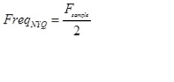
The clock jitter is often dominated by the wideband white noise floor of the ADC clock signal.
While the SNR performance of the ADC depends on various factors, the effect of the broadband jitter of the clock signal is given by the following equation:
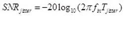
As shown, unlike a mixer, the SNR contribution from the clock jitter is directly proportional to the analog input frequency, fin, to the ADC.
When driving the ADC, the clock noise is limited by the bandwidth in the clock driver path , which is typically dominated by the ADC clock input capacitance. Broadband clock noise will modulate large input signals and will fold into the ADC output spectrum. The phase noise of the clock path will degrade the output SNR proportional to the amplitude and frequency of the input signals. The worst case is when a large high-frequency signal exists in the presence of a small signal.
In modern radio communication systems it is often the case that multiple carrier signals exist in the input and the individual signals of interest are filtered in DSP to match the bandwidth of the signal. In many cases a large unwanted signal at one frequency, will mix with clock noise and will degrade the available SNR at other frequencies in the passband of the ADC. In such a case the SNR of interest is the SNR in the desired signal bandwidth. In addition the SNRjitter value above is actually relative to the amplitude of the largest signal, often an unwanted signal or blocker.
The output noise in the desired signal band of interest is determined by:
a. Calculating the degradation of the ADC with a noisy clock and a large unwanted signal at a given input frequency, i.e., calculating the SNR in the full bandwidth of the ADC.
b. Using the ratio of the desired signal bandwidth relative to the full data converter bandwidth to calculate the SNR in the desired signal bandwidth.
c. Improving the value based upon the amplitude of the unwanted signal below full scale.
The result of step b is simply to modify the SNR equation given above as follows:

SNRj = SNR contribution of the clock jitter, into a bandwidth of fbw, in the presence of a large signal at frequency fin, with sample rate, fs
fin = input frequency of a full scale undesired signal, in Hz
Tjitter = input jitter of the ADC clock, in seconds.
fbw = bandwidth of the desired output signal, in Hz
fs = sample rate of the data converter, in Hz
SNRdc = SNR of the data converter with DC input, in dB
And finally, the maximum SNR available, in the signal band of interest with a full scale blocker present , is just the sum of the noise powers of the jitter and DC contributions.
For example, a 500-Msample/s data converter with an ENOB of 12.5 bits at dc, or equivalently 75 dB SNR is evaluated over a bandwidth of half the sample rate, at 250 MHz. If the signal of interest is 5 MHz wide, then the SNR possible near DC, in a 5-MHz bandwidth, with a perfect clock will be 75 + 10*log10 (250/5) = 92 dB.
However, the ADC clock is not perfect, and Fig. 3 shows the effect of degradation in the desired signal bandwidth of 5 MHz, as a function of a large undesired signal input at the frequency on the x-axis. The impact of the undesired signal is more severe as the clock jitter increases, and also as the input frequency increases. If the amplitude of the undesired signal decreases, the SNR available will increase proportionally.
For example, sampling a full-scale 5-MHz unwanted WCDMA signal at 200-MHz input, with a high-quality 500-MHz clock such as the HMC1034LP6GE with 70 fs of jitter when running in integer mode, then the SNR in a nearby 5-MHz channel would be about 91 dB. In contrast, if the clock jitter is degraded to 500 fs, the same data converter and signal would only exhibit an SNR of 81 dB, which represents a 10-dB degradation in performance.
Inputting the same signal into the data converter at 400 MHz, the 70-fs clock would yield an SNR of 88 dB. Similarly, with a 500-fs clock, the SNR value would degrade to just 75 dB.
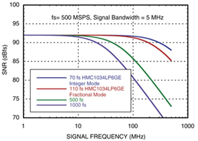
Fig. 3: ADC SNR vs. clock jitter and input frequency.
Selecting the right components for clock generation and data conversion enables a designer to extract the best performance from a given architecture. Important criteria to consider when choosing a clock generator are phase jitter and phase noise floor, which impact the SNR of the data converter being clocked. As the analysis indicates, the low-phase noise floor of the chosen clock generator as well as its low integrated phase jitter helps to minimize the SNR degradation at higher ADC input frequencies in multi-carrier applications. Both the HMC1032LP6GE and HMC1034LP6GE clock generators are designed with data converter applications in mind and work well with Hittite’s high-speed ADC devices. ■
Advertisement
Learn more about Hittite Microwave


