Surface-mount components are smaller than their lead-based counterparts and provide a radically higher component density. They are available in a variety of shapes and sizes designated by a series of standardized codes curated by the electronics industry. Of these components, the 0201-sized are the smallest, measuring 0.024 × 0.012 in. (0.6 × 0.3 mm) – that’s 70% smaller than the previous 0402 level! The 0201 components are designed to improve reliability in space-constrained applications such as portable electronics like smartphones, tablets, and digital cameras, but require delicate handling during the assembly process.
Given the miniaturized dimensions of an 0201 package, it is crucial that the mounting process abide by a series of guidelines regarding the design of the PCB mounting pads and solderable metallization, PCB circuit trace width, solder paste selection, package placement, solder paste reflow, solder stencil screening, and final inspection. It’s advisedable that one review this information when procuring the services of a PCB assembler. PCB assemblers such as Advanced Assembly typically have this information outline on their website or it can be obtained by contacting the sales department.

PCB solder pad guidelines
Two of the most commonly used PCB pad configuration for surface-mount packages are the solder mask defined (SMD) and the non-solder mask defined (NSMD). SMD pads include a solder mask placed over the margin of the metallization that restricts the solder paste’s flow on the top of the metallization and prevents the solder from flowing on the side of the metal pad.
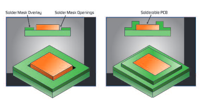 Alternatively, NSMD pads feature a solder mask that is pulled away from the solderable metallization. As a result, the solder flows around the sides and top of the metallization. NSMD pads are the favored variety of pad configuration in PCB design because the absent solder mask reveals more of the copper etching beneath, creating a larger opening around the metal pad which improves the solder joint’s reliability. The presence of the solder mask may cause package tilting when mounted to the board. Moreover, the copper etching exhibits a higher tolerance than the solder-masking process.
PCB solderable metalization
The three types of solderable coatings commonly used with PCB SMT devices are: Organic Solderability Protectant (OSP), electroless nickel/immersion gold (ENiAu), and Hot Air Solder Level (HASL).
A coat of OSP is typically between 0.25 and 0.35 microns thick; it is applied over bare copper features and helps reduce and retain the copper metallization for soldering. It also permits multiple passes through reflow ovens.
By contrast, the thickness of the ENiAu coat is determined by the maximum internal material stress and the temperature excursions the board will be subjected to througout its lifetime. The gold metallization cannot be allowed to surpass 5% of the overall solder volume or it will make the joint brittle. Lastly, the tin-lead HASL coat is not recommended for use with PCB pads as it is difficult to control the amount of solder applied to each pad, resulting in unevenly shaped pads.
But before a surface finish is selected, ensure that the land pands have a uniform coating to prevent the irregular surface plating, uneven solder paste thickness, and solder plate crowning from occurring.
PCB circuit trace width
The small size of the solder pad and the 0201 component causes the PCB to form a bump, making the component tilt and slide off the pad. Tilting can best be prevented by using a PCB circuit trace equal to the width of the mounting pad.
Solder selection
The most effective solder paste for 0201 components is type 4 or sphere-sized paste; pair the paste with water-soluble flux for cleaning.
Solder stencil screening/verificaton
Stencils are an effective way to accurately administer paste onto the PCB, and the suitable stencil thickness for an 0201-sized component is 0.1 mm. Ensure that the sidewalls of the stencil are tapered approximately five degrees and include an electro-polish finish to aid in discharge the paste once the stencil is removed.
Package placement
Automated pick-and-place equipment with magnification, a dual-image optical system, and a standard tolerance of ±0.05 mm is crucial when placing 0201 component packages. The dual-image system aids in aligning the bottomside of the package with the PCB’s pad.
Solder reflow
The profiles of 0201-sized components heading into the reflow oven should be verified on all new board designs, especially if there are multiple packages on the board. Solder paste manufacturers typically provide guidelines for the ideal profile along with any minor adjustments that must be made to account of the flux. The temperature of the devices should not be raised at a faster rate than 2°C/second during the early stage of the reflow.
Furthermore, the risk of voiding, or failure of the solder to thoroughly expel flux remnants during the reflow process, can be reduced by extending the length of time the components spend in the soak zone. Voiding is an anomaly that occurs with most SMT assemblies and is generally accepted when voids are small or the total amount of voided solder is minimal.
Advertisement
Learn more about Electronic Products Magazine


