By CHRIS SIEGL,
Member of Technical Staff,
Fairchild Semiconductor,
www.fairchildsemi.com
The definition of power factor (PF) is the ratio of the power drawn from the power grid (apparent power) to the power actually consumed in the load (real power). A power factor of ‘1.0’ is defined as a device consisting of a completely resistive load consuming all the power supplied to it. In the ideal case the ac-input voltage and current would be in phase and undistorted. In the case of pure sine waves when the current and voltage are in phase, the power factor is 1 (cos (0°) = 1).
As most switch mode power supplies (SMPS) draw a non sinusoidal current the wave shape must be corrected to minimize the input current distortion as well as phase correction. The key standard for power factor correction (PFC) requirements is European Union standard EN61000-3-2, which went into effect in 2001. It established limits on the harmonics of the ac input current up to the 40th harmonic. Using the right PFC greatly simplifies complying with this standard. Figure 1a shows the typical input circuit of a power supply without PFC. Figure 1b shows the resulting wave forms where the capacitor Cin is sized for a long hold-up time while operating with a light load. The capacitor discharge rate is low so conduction only occurs for a short time in the middle of the rectified-ac wave form, the rest of the time no current flows. The width of the current pulses will change as the load changes (discharging the capacitor during the voltage valley).
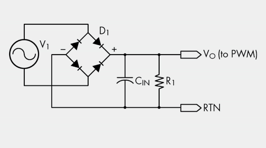
Fig. 1a: SMPS input without PFC circuit
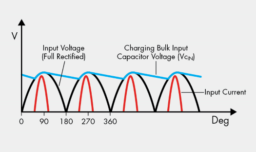
Fig. 1b: Voltage and current wave forms
So how is this short conduction time corrected? We need a better method to charge the hold-up capacitor for the SMPS while maintaining a sinusoidal current in phase with the input voltage waveform. To avoid those high current pulses in the center of each input voltage peak, the capacitor must be charged over the full voltage cycle. By always having the capacitor fully charged the size of this capacitor can also be reduced while still maintaining the same hold up time. Boosting the voltage to the capacitor to a voltage greater than the peak input voltage throughout the full voltage cycle can generate a current sine wave in phase with the voltage cycle and help the circuit approach a unity power factor.
Power correction using a boost converter
The boost converter is simple to implement and works well if modulated at a suitable frequency to distribute the current pulses throughout the voltage period. Figures 2a and 2b show the basic boost circuit and the waveform.
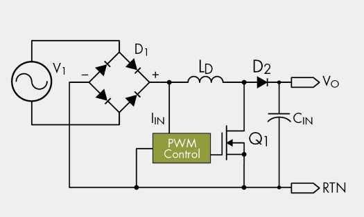
Fig. 2a: PFC Boost Circuit
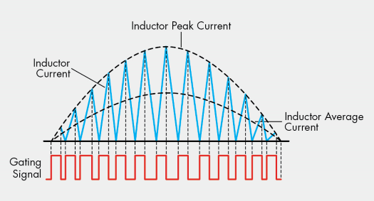
Fig. 2b: Discontinuous mode of operation
The wave form shows how this works in distributing current over the full voltage cycle. The operation shown is discontinuous mode where the boosting operation is performed through a series of current pulses shaping the average current. This is a proven approach for PFC and commonly used up to about 300 W. This solution has the disadvantage of needing large cores for the magnetics, having larger inductor current swings inducing greater skin effects resulting in higher losses in the inductors and requires larger input filters.
For higher power levels (greater than 300 W) the continuous conduction mode (CCM) is preferred. In this mode the current in the inductor does not reach zero during the switching cycle (see Fig. 3 ). The voltage swing is less than in discontinuous mode, while the ripple current is much lower. This results in much lower inductor core losses and a reduction in EMI which in turn reduces the size of the input filter needed.
The MOSFET in CCM is turned off and the flowing current flowing needs a very fast reverse-recovery diode to minimize losses during turn off. Some of the advantages to the CCM boost converter include the continuous input current in the boost inductor and the wide input range all the way to zero V. The inductor current ripple is reduced because the typical start current of each cycle is >0 A, which decreases the maximum peak current in the switching device. Control loops for average current mode keep the current proportional to the input voltage and voltage control loop regulates the boosted output voltage.
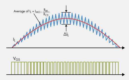
Fig. 3: CCM PFC mode of operation
PFC for higher power with interleaving
The interleaved boost PFC converter has become the topology of choice for high power applications due to the improved efficiency that can be achieved through load current sharing. By sharing the load current in more than one balanced phase, the rms current stress, current ripple, and boost inductor size per phase can be significantly reduced. Therefore, the maximum load efficiency can be significantly improved, which allows for the selection of cost effective power MOSFET and boost diode as well as improving longevity of the power supply by reducing component stresses.
A 3 channel CCM PFC controller
The latest generation of PFC controller from Fairchild, the FAN9673, can provide solutions of high-power PFC (above several kilowatts). It is a continuous conduction mode (CCM) PFC controller for a three-channel interleaved boost-type pre-regulator. This PFC controller incorporates the capability to implement leading edge, average current mode, and boost-type power factor correction, enabling the design of a power supply that complies with the IEC1000-3-2 specification. A key feature of the controller is an innovative channel management function, which allows the power level of the slave channels to be ramped up and down smoothly, controlled by the voltage on the channel-management (CM) pin, improving the PFC converter’s load transient response. Figure 4 shows a typical application circuit using the FAN9673 for a 5-kW PFC converter.
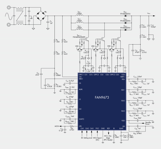
Fig. 4: FAN9673 based 3 channel interleaved 5-kW CCM PFC
A detailed reference design of this 5-kW application including layout details and magnetic design is available at
http://www.fairchildsemi.com/an/AN/AN-FEBFAN9673_B01H5000A.pdf
Advertisement
Learn more about Fairchild Semiconductor


