The right MCU architecture for your embedded design
A brief look at some popular formats
BY SHAWN PRESTRIDGE
IAR Systems
Foster City, CA and Uppsala, Sweden
http://www.iar.com
So many different microcontroller architectures are on the market today that an embedded engineer faces a daunting task when trying to find the right one to satisfy the needs of a design. That selection is a bit like writing a paper for your English class: There are no right or wrong answers, but some choices are clearly better than others. This article explores just three popular architectures and their attributes. This is by no means intended to be a definitive listing, but rather a brief survey of some available types.
The ARM architecture
The ARM MCU architecture, a 32-bit MCU renowned for its simplicity, power, and speed, has taken the embedded world by storm. Its many different flavors include the ARM7, ARM9, and ARM11, but the push is to move toward newer ARM cores, called A, R, and M the A targeting applications, the R real-time processing, and the M more traditional MCU uses. The letter is followed by a number indicating the relative power of the core to others in the line. The first in the Cortex lineup, the M3, is produced by many different silicon makers like Atmel, NXP, STMicroelectronics, and Texas Instruments, each putting on its own mix of peripherals.
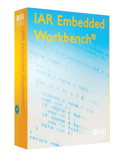
Fig. 1. Embedded Workbench is an example of a tool set for building and debugging embedded applications using assembler, C, and C++.
A lower-powered variant of the Cortex M3 is the M0. On the application side (running at higher DMIPS) are the A5, A8, and A9, exceedingly popular in mobile phone applications. For example, TI’s popular OMAP chip is a dual-core DSP and A8 bundled together to handle cellular communications and PDA functions.
The A9 allows for multiple cores for ultra performance. Lastly, the R4 is targeted toward so-called “deeply embedded” applications where the footprint of the core is an issue. The R4 targets users who need mid-level performance. There is a litany of hardware and software tools for developing with the ARM architecture which certainly fuels its popularity, including IAR Systems, GNU, and Green Hills.
The MSP430 architecture
Another popular architecture is the Texas Instruments’ MSP430. It’s a 16-bit architecture featuring very low-power, with standby currents less than 1 µA and wakeup times less than 1 µs. Since the early 1990s, when the 430 was introduced, TI has billed it as “The world’s lowest power MCU,” a claim that stood largely unchallenged until the last couple of years.
The 430 has several generations which were developed in the order of 3xx, 1xx, 4xx, 2xx, and finally 5xx. The number indicates the included peripherals and roughly indicates the physical size of the chip. The 1xx series sports up to 60 Kbytes of flash and 10 Kbytes of RAM and has analog comparators, DMA, hardware multipliers, SVS, and a 12-bit DAC. The 2xx series are similar to the 1xx but are lower-powered and have op amps and more accurate on-chip clocks, with flash sizes up to 120 Kbytes and up to 8 Kbytes of RAM.
The 3xx has up to 32 Kbytes of ROM and 1 K of RAM and sports an embedded LCD controller and HW multiplier. The 4xx series is very similar to the 2xx except that it offers the LCD controller and USCI modules.
The latest in the lineup is the 5xx series similar to the 4xx but with USB capability. It the lowest power series of the family. Popular applications include situations where the processor spends most of its time sleeping and wakes up for a short period of work. The 430 is supported by several different hardware debuggers such as the TI USB FET Debugger and the Olimex MSP430-JTAG and three major compilers: IAR Systems, TI’s Code Composer, and GNU.
The AVR architecture
Still another popular architecture is the 8-bit Atmel AVR, a modified Harvard architecture that was one of the first microcontrollers to incorporate the use of flash memory in its package. These devices are easy to understand and program and are used in a wide variety of applications.
This family comes in three basic groups, the Atmel tinyAVR (ATtiny), the Atmel megaAVR (ATmega) and Atmel XMEGA (ATxmega). The ATtiny has a limited peripheral set with up to 16 Kbytes of memory, but comes in a very small package: from 6 to 32 pins. The ATmega series is wildly popular due to its extensive peripheral set and up to 256 Kbytes of memory with packages from 28 to 100 pins. The ATxmega series is similar to the ATmega series but also boasts DMA, high-speed 12-bit ADC and DAC, an event system that allows peripherals to communicate without the CPU, 1.6-V operation, and AES/DES cryptography.
The typical clock speed for an AVR is up to 20 MHz, but some devices can be pushed as high as 32 MHz. The AVR’s RTC power-save mode is as low as 550 nA. Most debugging for the AVR is done via an AVR Dragon or an Atmel JTAGICE mkII. These debuggers are generally coupled with one of two major IDEs to complete the toolset, namely IAR and GNU/AVRStudio. The low cost of the AVR series and its associated tools makes the AVR very popular with hobbyists and kit developers as well as professionals looking for dynamite in a small package. ■
Advertisement
Learn more about IAR Systems


