By Eileen Sun, GLF Integrated Power
Designers of wearables — including smartwatches, fitness trackers, heart monitors, and many other devices — are constantly trying to find ways to increase battery life in order to improve user convenience. Yet for all of the advances that have been made in their design and capabilities, wearables often require frequent recharging. This is because most wearables are using the same load switches designed for bigger devices like tablets, which have much larger battery capacity than wearables, and where battery-draining leakage current and ON resistance are less of a concern.
To address this challenge, new ultra-low leakage current load switches are setting the standard for efficient power management in wearable devices. By using advanced load switches, efficiency can be dramatically increased. These savings will translate into either a smaller battery or a longer battery life and will differentiate wearable products in a very competitive market.
Battery efficiency in wearables
In wearable products, load switches perform the essential battery-management tasks with minimum footprint and nearly zero leakage current and/or ON resistance. However, IC load switches that are meant for laptops and tablet computers simply can’t meet these demands.
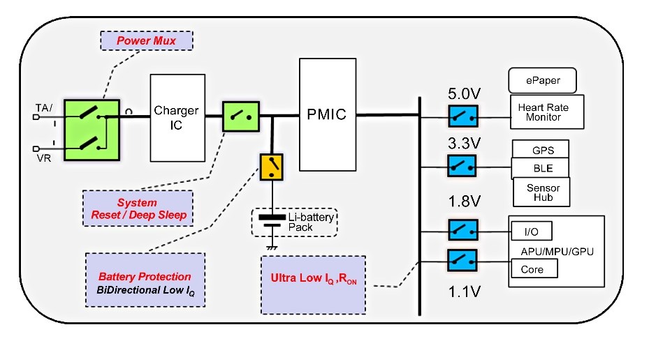
An example of a typical wearable application (Fig. 1 ) includes several environmental sensors, GPS, display, memory, wireless connectivity, and a fast, feature-rich microcontroller (MCU). In order to extend battery life, the circuitry includes a number of load switches to turn on devices sequentially or place the device in “sleep” mode and to turn off functions as needed.
In this respect, the example shown in the block diagram is not materially different than that of a typical handheld tablet or mobile phone. The difference lies in the size and performance of these devices.

Fig. 1: New high-performance load switches can add hours or even days to wearable battery life.
Many of the functional devices utilized in wearables (including connectivity, sensing, and MCUs) come with power-saving modes that offer developers a false sense of lower-power control. Table 1 shows examples of low-power mode current drawn by a typical mix of ICs and modules.
Table 1: Typical low-end wearable functions and the power they draw.

Table 2 describes the current drain of other features required in higher-performance applications. Together with the MCU/APU and other devices, standby current can really add up. All of the required features can turn a device into a “power monster.”
Table 2: Typical devices that do not offer the needed low standby current.

Criteria for choosing a load switch
Designers of wearables need to consider load switch selection criteria. The following are examples to compare the performance of available devices.
Mostly ON vs. mostly OFF
Depending on whether the subsystem is ON or OFF, different parameters of the load switch become important. Most switches are optimized for one but not for both conditions.
In the case of a “Mostly OFF” subsystem, the current standby ISD (standby current leakage) becomes the most important parameter to consider. The best devices on the market are well under 1 μA. Table 3 includes devices that meet this criterion. Marking a significant improvement, the table shows that an advanced low-leakage current load switch, GLF71301 device, offers best-in-class ISD at 7 nA.
Table 3: GLF load switch’s IQ and ISD performance compared to competitive devices.

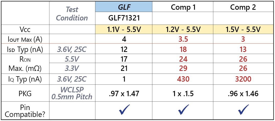
If the subsystem is “mostly ON,” then the ON resistance of the switch, RON , becomes paramount. A designer should look for a RON of less than 100 mΩ at the max operating range. Table 4 offers a sampling of some of the devices offering the lowest RON . As shown, the GLF71321 load switch offers the best RON performance (17 mΩ at 5.5 V and 21 mΩ at 3.3 V).
Table 4: GLF load switch’s RON performance compared to competitive devices.

Voltage range
Most wearables have several different voltage rails ranging from 1.1 V for the CPU core to 5.0 V for higher-voltage peripherals. A load switch with a wider range of voltage rail options can help manage inventory and used throughout. All of the devices listed in Tables 3 and 4 meet this criterion.
It should be clear from the information presented in these tables that both ISD and RON will have a significant effect on battery life. Another factor to take into account is the quiescent current (IQ ) of the device. This is the “overhead” current drawn by the device when in the “ON” state. A quick review of these same two tables reveal that the GLF devices are up to several hundred times lower than the others.
The future of wearables
It is estimated that by 2025, there will be over 1 trillion IoT devices in operation; of these, a significant portion will be of the wearable variety. Consumers will continue to expect wearables to need less-frequent charging. This, in turn, will make it necessary for applications engineers to employ the most battery-efficient design techniques possible.
Selecting the latest ultra-low leakage current load switches offer designers an effective means for improving battery life in wearables. Unlike conventional devices more suitable to larger portable electronics, these wearable-optimized load switches can easily extend operating time from days to weeks between recharging.
Advertisement


