The transformation of silicon to system design
Changes in system development require EDA to evolve further
BY CHARLIE HUANG
Cadence Design Systems, San Jose, CA
http://www.cadence.com
Truly inspired electronics products are in demand and delivering profit, even in a down economy. Consumers are delighted by products like Apple’s iPhone and iPad, which mark a new era for product innovation and changed how systems are developed. Google and its Android platform have added to the trend, further emphasizing that software is becoming the key driver in both the value and design chains. These new products have redefined the economics and market for electronics, and suggest fresh opportunities for the industry.
To keep pace, the industry needs a new approach to system development. It must adopt integrated system-level development that takes a 360° view of hardware, software, and the integration of all forms of intellectual property (IP).
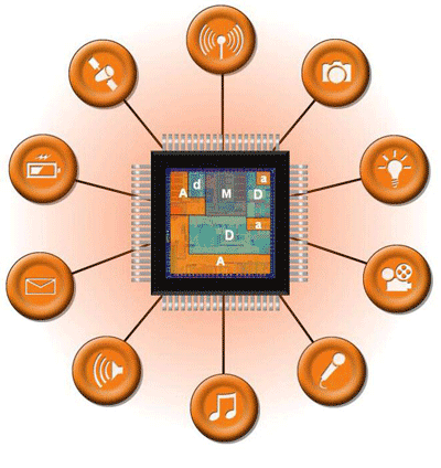
The underlying engine that enables this innovation has traditionally come out of the EDA industry. EDA was created to increase productivity of electronics engineers as they tackled ever more complex design tasks. As the semiconductor industry grew and chips became smaller and more dense, the EDA industry changed to help engineers manage complexity that strains human comprehension. Changes in system development require EDA to evolve further. Teams of engineers need to easily design and combine reusable hardware design components to create new silicon devices, build hardware and software in parallel, and develop software with hardware awareness. These changes also require that EDA develop to a level where a specification of IP can be converted into correct hardware automatically, freeing more time for specification development and system-level design. The savings in design schedule and resource costs can then be used to provide customers with rapid delivery of systems.
Silicon devices are often made from multiple existing IP building blocks and a few modified or new IP blocks. Reusing IP must become less of a burden so that the architect can focus on the conceptual work of creating the system, not the detailed work of the connections. The designers must be allowed to concentrate on performance, power consumption, and packaging cost. The electronics industry and EDA must simplify and standardize a methodology for IP creation that allows this level of automated reuse and resulting silicon development cost savings.
The embedded software that goes with the hardware must be developed earlier in the project. Yet a serial approach to software and hardware development persists today, with the exception of a few well-formed ecosystems such as the iPhone and Android. For nearly all other system products, the embedded software cannot be designed without considering the capability of the hardware and vice versa.
In some systems, performance and power needs dictate that some functionality be implemented in hardware. To integrate such hardware-based functionality into the overall device, communication protocols are designed into the silicon and incorporated into embedded software. These interactions are complex and must be optimized to meet the overall performance and power needs of mobile or other consumer products.
The interdependence of software development on hardware complicates the system design process because there is not always a way to meet requirements without changing the hardware — it’s an iterative process. The EDA-enabled hardware development process therefore must support iterative approaches to facilitate rapid software development and nimble hardware implementation.
For traditional semiconductor companies, these trends lead to burgeoning software teams that are frequently larger than the hardware teams. The companies need EDA solutions to deliver in ever-shorter schedules and still contain the costs of both software and hardware development. More important, their systems customers are often developing pure application software, and they demand that the semiconductor company deliver a software-programming interface for the silicon device — a layer of abstraction that completely hides the hardware part of the system. This puts even more pressure on the semiconductor provider to deliver any required hardware change quickly, as if it were simply another software component.
None of these transitions will be easy. Change is occurring in the marketplace. System project managers often promote a software-centered product strategy, which demands a design methodology for timely and successful execution. Semi and EDA industries have an opportunity to capitalize on these trends and create sustainable differentiation, which is the golden goose of high-technology companies. ■
Advertisement
Learn more about Cadence Design Systems


