Thermal simulation is an integral part for developing power products and for providing product material guidance
BY SANMUKH PATEL and GERRY BALANON
Texas Instruments
Dallas, TX
http://www.ti.com
The trend in end-equipment design is to optimize the module profile for sizing. This introduces a migration from metal heat sinks to PCB copper plane-based thermal management. Today’s modules use lower switching frequencies for switch mode power supplies and large passive components. Linear regulators are inefficient for voltage conversion and quiescent currents to drive the internal circuitry.
Thermal simulation at the IC level and system level is important as equipment designs become compact with increased functions and performance.
For applications with operating ambient temperatures ranging from 70 to 125C, and up to 140C in some specific automotive applications in bare die form, it is important that the system operates without interruptions. Accurate thermal analysis of both the application’s transient and static worst conditions is becoming more important for optimizing electronic designs.
Thermal management
The challenges in thermal management are to meet the shrinking package size with better thermal performance, higher operating ambient temperatures, and smaller budgets for copper heat planes. High packaging efficiency leads to a high concentration of heat producing elements, resulting in very high heat flux at IC and package levels.
Factors considered in a system are other power devices on the printed circuit board that may influence the temperature of the device under analysis, system space and airflow design/constraints, etc. Three levels are considered for thermal management: package, board, and system (see Fig. 1 ).
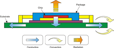
Fig. 1. Typical heat transfer path in an IC package
Low cost, small form factor, module integration, and package reliability are considerations in selecting packages. With cost as a key consideration, lead-frame-based thermally enhanced packages are gaining popularity. This includes heat slugs or exposed pad and heat spreader type packages, designed to improve thermal performance. In some surface mount packages, special lead frames fuse several leads on each side of the package to act as heat spreaders. This provides good thermal path for heat transfer from the die pad.
IC and package thermal simulations
Thermal analysis requires detailed and accurate models of the silicon product and case thermal properties. The semiconductor supplier provides silicon IC thermal and mechanical properties and packaging, while the equipment manufacturer supplies information about the module materials. The product user provides the environmental information.
This analysis helps IC designers optimize power FET sizing for worst-case power dissipations in both transient and static modes of operation. In many power electronic ICs, the power FETs constitute a large percentage of the die area. The thermal analysis helps to optimize their designs.
The selected package typically has a metal area exposed to provide a low thermal resistance path from the silicon to the heat dissipater. Key parameters required for the model are as follows:
• Silicon die size aspect ratio with die thickness.
• Power device area and location, and any supporting drive circuitry that contributes to heat.
• Power structure thickness (diffusion within silicon).
• Die attach area and thickness for the silicon attachment to the exposed metal pad or tab. May include percentage voiding of the die attach material
• Area and thickness of the exposed metal pad or tab.
• Package size with mold compound and connection leads.
Thermal conducting properties are required for each material used for the model. This input should also factor in any temperature dependency variations for thermal conductivity including:
• Silicon thermal conductivity
• Die attach, mold compound conductivity
• Metal pad or tab conductivity.
Package product and PCB interaction
A critical parameter for thermal simulation is to determine thermal resistance from pad to heat-sink material. Several methods to consider are:
• Multilayer FR4 board (four and six layers are common)
• Single-sided board
• Top and bottom layer boards
Heat extraction and resistance paths vary, depending on the implementation can be:
• Thermal vias from heat pad or tab attached to the inner heat-sink plane. Use solder to connect the exposed pad or tab to the PCB’s top layer.
• An opening on the PCB underneath the exposed pad or tab can contact a protruding heat-sink pedestal connected to the module’s metal case.
• A heat sink on the copper-plane on the top or bottom sides of the PCB that connects the heat sink plane to the metal case with a metal screw. Use solder to connect the exposed pad or tab to the top layer of the PCB.
Additionally, the weight or thickness of copper plating used on the PCB for each layer is key. For thermal resistance analysis, the layers attached to the exposed pad or tab are directly impacted by this parameter. This is typically the top, heat sink and bottom layers in a multi-layer board.
In most applications, these are either two ounce copper (2 oz Cu = 2.8 mils or 71 µm) outer layers with 1-oz copper (1 oz Cu = 1.4 mils or 35 µm) inner layers, or all 1-oz copper layers. In consumer applications, some may even use 0.5-oz copper (0.5 oz Cu = 0.7 mils or 18 µm) layers.
Model information
An IC floor plan is required to simulate die temperature. This consists of all the power FETs on the die, and practical location to meet the bonding guidelines for packaging.
The size of each FET and the aspect ratio for heat distribution is important. Another important factor to consider is whether or not the FETs are powered simultaneously or sequentially. Model accuracy is dependent on physical data and material’s properties being used.
Static or average power dissipation analysis in the model requires less computation time and converges once the highest temperatures are recorded.
Transient analysis requires power versus time profile. The data are recorded with much finer resolution steps than the switching power profile to accurately capture the peak temperature rises during a fast power pulse. This analysis generally takes longer and requires much more data inputs than a static power simulation.
The model could simulate epoxy voiding at the die attach region, or solder voiding at the PCB thermal land interface. In both cases, epoxy/solder void impacts the thermal resistance on the package (see Fig. 2 ).
Thermal definitions
θja – represents the die junction to ambient resistance, generally used for thermal package performance comparisons.
• θjc – represents the die junction to case top resistance.
• θjp – represents the die junction to exposed pad resistance, generally used for good reference to predict die junction temperature.
• θjb – represents the die junction to board below one lead resistive path.
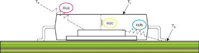
Fig. 2. Thermal resistive path for heat transfer.
Implementing the PCB and module casing
Data indicates that minor modifications may be required to reduce the FET’s maximum temperature on the die near the top to prevent the hot spot from exceeding the T-junction of 150C (see Fig. 3 ). The system user has options to control the power profile for this particular sequence to reduce the power temperature on the die.
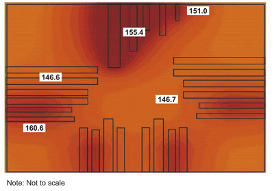
Fig. 3. Example of a result from thermal simulations
Thermal simulation is an integral part of developing power products. It also provides guidance of thermal resistance parameters from silicon FET junctions to implementing various materials in the product. Systems can be optimized for each application – once the different thermal resistive paths are understood.
Also this data can be used as a guideline for correlation with any de-rating factors with an increase in ambient operating temperature. The results are used to help the product development teams with their designs.
For more information about packaging and thermal reference information, visit http://www-s.ti.com/sc/techlit/slma002.pdf.
Advertisement
Learn more about Texas Instruments


