Thin-film chip resistors use sputtered Nichrome-based terminations
BY BRIAN MCCABE and KORY SCHROEDER
Stackpole Electronics, Raleigh, NC
http://www.seielect.com
Current downsizing trends have pushed resistor technology to its limits. For example, packaging alone for an 0201size chip resistor is roughly 60% of the total part cost. Chip arrays can help ease the placement and packaging issues for some designs that use the same resistance value in the same proximity on the circuit board. However, this doesn’t work for everyone.
Recent developments in thick-film and thin-film technologies enable higher power ratings in a given chip size. It is well known that thin-film resistive elements provide a number of performance benefits over their thick-film counterparts, while the only clear advantage for thick-film resistors has been cost.
That significant cost differential may be greatly reduced with the latest materials and process advances, which promise to have a substantial impact on the commodity chip resistor market. It is now reasonable to expect commodity thin-film chip resistors, with tolerance of 1% and a temperature coefficient of resistance (TCR) of ±100 ppm/C, to be priced in the same general range as a thick-film resistor of comparable precision.
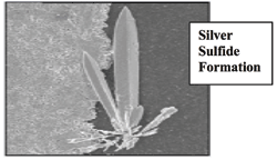
In high-sulfur environments such as automotive, industrial, and heavy agricultural and construction equipment, typical commodity thick-film chip resistors will begin to experience resistance shifts due to the formation of silver sulfide. The sulfur diffuses through the plating and barrier layers to the silver, forming silver sulfide (see Fig. 1 ).

Fig. 1. Sulfur diffuses through the plating and barrier layers to the silver, forming silver sulfide.
Silver sulfide is nonconductive and with continued exposure to sulfur will mean an increase in silver sulfide formation until all of the silver has been completely changed into silver sulfide. The conductive layer will be interrupted and the part will become open. This is a particularly frustrating phenomenon for any automotive or industrial equipment manufacturer because it is a latent failure that is completely undetectable at the time of manufacture. Some automotive and industrial equipment manufacturers have had success in thwarting this silver sulfide formation by potting their electronics, but this is not feasible for all applications and is not a guaranteed reliable method of preventing sulfur contamination.
Thick vs. thin
Commodity thick-film resistors typically have inner terminations of printed silver / palladium of varying levels. These less-expensive termination materials have a higher level of silver, but it is typically the silver in the inner termination that is susceptible to contamination by sulfur.
It is possible to find thick-film materials that have a decreased amount of silver, but to date, these alternative materials are higher in cost such that their mass implementation seems unlikely. Thin-film chip resistors, on the other hand, have a sputtered Nichrome-based inner termination that is free of silver and usually any other precious metal. This means that the pricing for thin-film Nichrome-based materials is less volatile than those thick-film materials containing increased amounts of gold, palladium, or platinum.
Only chip resistors without silver- or copper-based materials in their inner terminations, or that have their inner terminations protected by an intermediate layer of sulfur impervious material, are completely immune to sulfur contamination. There are competitive thick-film-based solutions in the market that are generally regarded as sulfur resistant, but they too will experience sulfur contamination and, given enough time, will eventually fail as an open circuit.
It is also known that misalignment in the printed protective passivation layer may lead to an increased susceptibility to sulfur contamination. In those cases, slowing down the printing processes will minimize this effect, but that also raises manufacturing costs and reduces manufacturing throughput. Since thin-film inner terminations do not have susceptibility to sulfur contamination, this process accuracy is not critical.
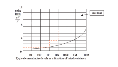
Clearly thin-film resistor technology, in terms of its inner termination, withstands sulfur better. Beyond that, thin-film technology resistors also have overall stability, lower noise, and lower stray capacitance and inductance (depending on resistance value). Figure 2 shows a typical thin-film resistor has a dramatic improvement over thick-film chip resistors, especially at higher resistance values.

Fig. 2. Typical current noise levels as a function of rated resistance.
In the past, this improved response with lower electrical noise was only important in high-end audio applications. However, now the latest high-speed communications devices such as routers, bridges, and DSL modems are beginning to move beyond the noise capabilities of thick-film resistors. Thick-film resistors are noisier for a variety of factors, but one of the most apparent areas where thin-film and thick-film technologies differ is in their laser trim properties. Once fired, thick-film materials are glasslike in nature. As a result, laser trimming forms many small microcracks around the trim as the material cools down. These microcracks are a source of parasitic capacitance and false current paths, all yielding an inherently lower performance for high-speed communications signals.

Fig. 3. Power ratings and EIA standard chip resistor sizes
To reduce the effects of laser trimming on thick-film elements, manufacturers typically add a dielectric glass layer to stabilize the laser trim. This layer contains trace amounts of lead, and is understood to be critical to the long-term reliability of thick-film resistors, so much so that this dielectric glass layer is given an exemption from RoHS at this time.
However, in the future, it is unclear whether this exemption will be carried on or if the industry will demand an alternative method of laser trim stabilization that doesn’t contain lead. Thin-film technology can provide a “greener” or more environmentally friendly resistor because the lead-containing glass used on nearly all thick-film chips is not needed.
Developments
One of the most recent developments in thin-film technology, as well as thick-film, is the ability to obtain higher power ratings for a given EIA standard chip resistor size (see Fig. 3 ). This critical development allows engineers to downsize their design without sacrificing power handling. This breakthrough is critical for enhancing current designs and to size reduction for future designs, allowing for smaller end products or for increased features in the same size product.
The most critical factor hindering thin film’s mass acceptance as a commodity chip resistor has been its cost. Typical pricing for the poorest tolerance and TCR thin-film chip resistor has been ten times to a hundred times more expensive than its closest thick-film counterpart. To reduce this discrepancy, suppliers were required to completely redesign the thin-film materials for high-speed low-cost manufacturing. It also required developing a high-speed inline thin-film manufacturing process. The final step to lower cost was loosening the requirements of the thin-film materials from precision levels (0.1% tolerance and 25 ppm TCR or better) to commercial, general purpose, and commodity levels (1% tolerance and 100 ppm). These three advancements together can be incorporated into a chip resistor priced within 10% to 20% of typical commodity thick-film chips. That may be the most compelling development of all. ■
Advertisement
Learn more about Stackpole Electronics


