Researchers from the Karlsruhe Institute of Technology (KIT) in Germany have developed an innovative photo detector for optical data paths — the central component at the receiver side of the glass fibers — that sets new standards to their size. The researchers said the footprint of less than 100 square micrometers is suitable for integration in an integrated circuit, on top of its impressive data rate.
The photo detector permits a significant performance increase of optical communication systems because they can be integrated on optical semiconductors in large quantities. During experiments, the researchers reached a throughput up to 40 Gbps, which is enough to transfer the entire content of a DVD within a fraction of a second.
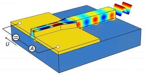
Pictured above is the plasmonic detector, which is coupled directly to a silicon optical waveguide and less than one micrometer in size. Image source: KIT.
“This plasmonic internal photoemission detector (PIPED) is the smallest detector ever to reach this data rate,” said Sascha Mühlbrandt, researcher at the Institute for Microstructure Technology and the Institute for Photonics and Microstructure Technology. The device is 100 times smaller than a conventional photo detector.
A major benefit of this small size lies in the possibility that the photo detector can be integrated along with downstream preprocessing circuitry on a single CMOS chip. According to the team, the introduction of novel plasmonic components for high-speed data exchange between integrated circuits in computers opens the possibility to combine the advantages of electronic and optical components at the same or higher data throughput as with electronic-only components, said project coordinator Manfred Kohl from the KIT Institute for Microstructure Technology.
The detector was developed within the project NAVOLCHI (Nano Scale Disruptive Silicon-Plasmonic Platform for Chip-to-Chip Interconnection) which has been funded from the 7th EU Research Frame Program.
To combine the optics and electronics within tiny spaces, the photo detector makes use of surface plasmon polaritons, which are highly concentrated electromagnetic waves on metallic-dielectric boundary surfaces. “This new class of plasmonic converters is based on the driect signal conversion at metallic surfaces at optical wavelengths, known as photo emission,” said Mühlbrandt. “To efficiently control the absorption of light and its conversion into electric signals, the researchers generated charge carriers in a titanium-silicon junction and recombined in another gold-silicon junction. The high speed of the detector is achieved through its specific geometry — between the two metal-silicon junctions there is a distance of less than 100 nanometers.”
The researchers regard the PIPED concept only as essential for future optical data transmission systems but also as key component for wireless data communications.
Source: EE Times
Advertisement
Learn more about Electronic Products Magazine


