By Majeed Ahmad, contributing writer
NAND flash technology is on a roll with advancements in cell structure and the subsequent boost in storage density. That allows this non-volatile-memory (NVM) chip to deliver faster throughput and higher bandwidth at the system level while significantly reducing the die size.
In other words, innovations in the NAND flash realm are keeping pace with the escalating demands in today’s data-centric world in which high-capacity storage is required to process, store, and manage large volumes of information at higher speed and lower power consumption.
The next-generation NAND flash chips will be deployed in solid-state drives (SSDs) for use in data centers as well as in enterprise and consumer SSDs, tablets, smartphones, and memory cards.
Here, it’s worth mentioning that back in 2000, when the first NAND flash-based USB drive was introduced, we measured storage density in megabytes (MB). In less than two decades, relentless innovation and thriving storage demand have taken capacity to 64 gigabytes (GB) in a single NAND flash chip. And while storage density is constantly increasing, the cost per GB is coming down at the same time.
This article scouts the current NAND landscape to find out what’s driving innovation in the golden age of flash memory enabling denser storage in smaller sizes. It inevitably starts with the transition to 3D NAND flash technology that industry observers call a defining moment for the memory business.
The advent of 3D NAND flash
The migration from 2D planar NAND to 3D NAND essentially began during the mid-2010s. At that time, NAND flash technology looked to be in terminal decline because of scaling challenges.
For many years, chipmakers could increase the capacity of NAND flash memory by shrinking the design rule and manufacturing process node. However, it was becoming extremely difficult to further increase memory capacity using the conventional planar NAND flash memory technology.
The shrinking lithography — manufacturing chips on a smaller scale — merely put NAND flash cells too close to each other, leading to issues like interference and current leakage. So memory suppliers began to stack layer upon layer of flash cells atop one another for creating denser and faster NAND chips.
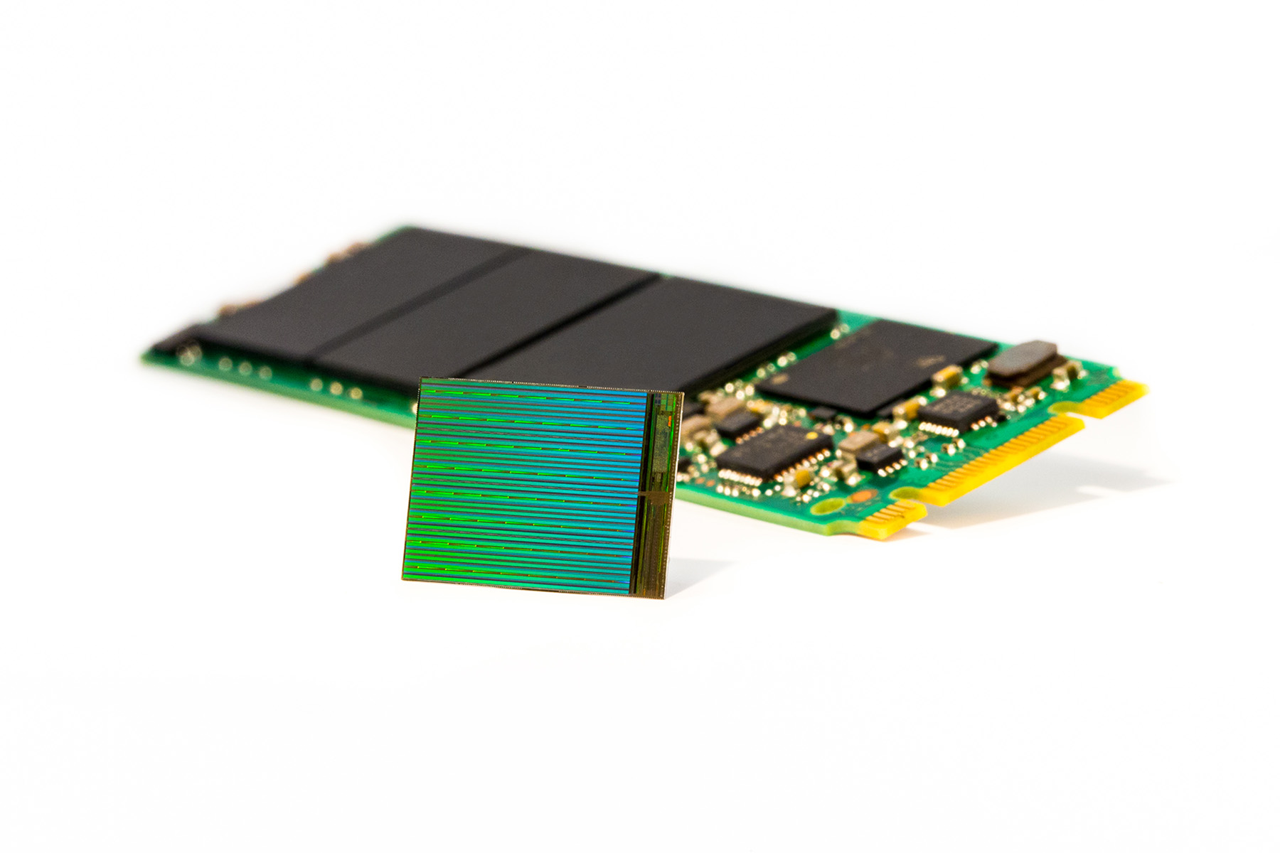
Fig. 1: The 3D NAND flash chip shown here inside an SSD provides three-times-higher capacity than a planar NAND flash chip. Image Source: Micron.
In 2007, NAND flash inventor Toshiba Memory released the first prototype of its 3D flash memory technology: BiCS FLASH. Fast-forward to the fourth quarter of 2017: 3D NAND flash memory accounted for more than 80% of Samsung Semiconductor’s production of NAND flash chips.
However, the buzz surrounding 3D NAND flash is still high because the memory technology is still in the early stages. As the number of stacked layers increases, issues like flash cell size, cell efficiency, and manufacturing yield become crucial. Moreover, 3D NAND flash chips mandate huge investments in fabs, which are currently in the buildup process.
Other innovations are also being built upon the 3D NAND flash infrastructure. For example (as explained later in this article), 3D NAND flash lays the foundation for bringing back lifecycle endurance to multi-level-cell (MLC) chips, which are otherwise struggling to maintain reliability due to current leakage and bit errors.
More importantly, a key milestone alongside the advent of 3D NAND flash is advancements in the stacking structure of these memory chips.
The 96-layer NAND structure
NAND flash suppliers like Toshiba are now showcasing 96 layers of vertical storage capability that reduces the cost per bit and increases the manufacturability of memory capacity per silicon wafer. The third-generation 96-layer 3D NAND structure provides a 50% increase in the number of layers currently used in most NAND flash chips. And so far, it’s progressing quite well.
The NAND flash chips, featuring 96 active-word lines or layers, can condense even more data into smaller spaces and unlock new storage workloads. But how does the 96-layer stacking process work? The 3D flash stacks are built in channel holes etched into a stack of memory layers on top of silicon substrates.
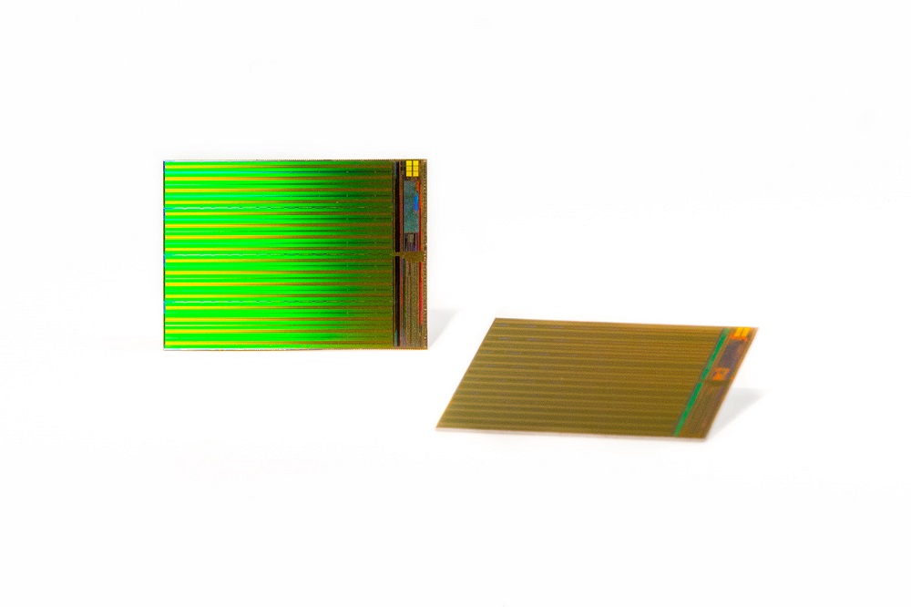
Fig. 2: The 96-tier NAND flash structure provides a significant increase in the number of layer stacks. Image Source: Micron.
However, when the number of layers surpasses 64, flash technology challenges such as current density, cell uniformity, and aspect ratio of channel hole become critical. Manufacturability and yield issues also become big challenges as the height of stacks increases.
Like 3D NAND flash, it’s another way of packing even more data via a stacked structure and creating new operating points for storage density. However, just like the 3D NAND flash undertaking, yield maturity is crucial in the success of 96-layer NAND flash chips.
For now, flash suppliers are using the 96-layer 3D NAND memory in economical flash drives and memory cards sold in retail segments. However, once memory chipmakers figure out how to produce the 96-layer 3D NAND with sufficient yields, these flash chips could find a place in the enterprise- and client-grade storage devices.
From TLC to QLC
Another bright spot in NAND’s technology journey is the commercial realization of quadruple-level-cell (QLC) memory chips that led to 33% higher array density compared to triple-level-cell (TLC) flash chips. Unlike TLC memory chips, which store 3 bits per cell, QLC flash chips store 4 bits per cell to achieve as much as one terabit density per die.
That takes NAND flash to new storage frontiers like read-centric workloads that have traditionally relied on massive arrays of hard disk drives (HDDs). Not surprisingly, therefore, memory chipmakers like Micron Technology Inc. are advocating that 4-bits-per-cell flash chips reaching the density of 1 terabit can replace HDD arrays in storage applications in which data is occasionally written while it’s read and analyzed more frequently.
Workloads such as big data, content delivery, machine learning, and real-time analytics perfectly fit into this storage description. That, in turn, allows data centers to pack more storage at less cost and lower power consumption as compared to slow and power-hungry HDDs.
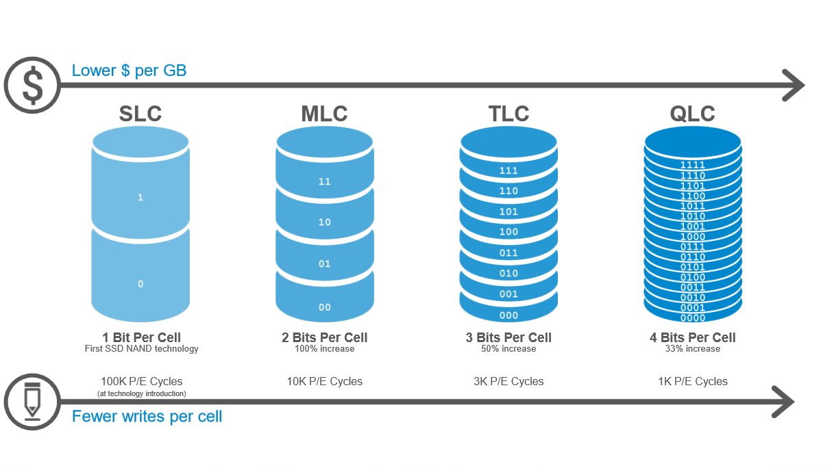
Fig. 3: This is how QLC memory chips offer more density per NAND flash cell. Image Source: Micron.
The 4-bits-per-cell NAND is optimized for read-intensive, performance-sensitive workloads for enterprise flash storage in data centers. In other words, HDDs, the last bastion of rotating media developed nearly a half-century ago, are in the crosshairs of NAND flash technology.
The multi-level-cell NAND has been one of the most profound tenets of flash innovation because it offers greater density than single-level-cell (SLC) flash chips. However, unlike first-generation SLC flash chips, MLC flash is hindered by low-write capability. As a result, the SLC flash chips are seen as more reliable.
The workaround has been centered on using wear-leveling algorithms in MLC flash chips to bring them on par with HDDs in terms of longevity. And for SSD solutions in cloud and data center environments, they efficiently serve the read-centric workloads with fast and reliable data access.
Intel and Micron, jointly developing 3D NAND flash products, claim to have qualified the industry’s first 4-bits-per-cell 3D NAND on a 64-layer stack. That, according to the two chipmakers, leads to the industry’s highest Gb/mm2 density.
The drive for improvements in NAND flash is irreversible, and it’s apparent from the expansion in production capacity for NAND flash chips taking place from 2018 to 2020. The storage needs of the emerging workloads in the cloud and data center environments make the technology shifts in NAND memory inevitable.
Advertisement


