Embedded designers have implemented heterogeneous architectures since the advent of commercially viable FPGAs. Initially, FPGAs acted primarily as glue logic for an interface between processing systems, peripherals, and I/O. But as FPGA technology improved, the market expanded to play a larger and more central role in embedded systems. The latest trend in heterogeneous computing is to integrate processor and FPGA subsystems into a single SoC. Processor and software-centric design teams can now take advantage of both systems on these complex SoCs.
A heterogeneous computing architecture
System designers are attracted by the combination of processor and FPGA for embedded systems because of the flexibility and performance they offer in a standard design template. The processor in the system provides a wide range of standard peripheral interfaces, such as Ethernet, serial, USB, CAN, SPI, and memory. In a processor-only approach, application I/O is typically interfaced via SPI or USB. Developing software for the processor is widely understood and manageable.
Placing an FPGA between the processor and the application-specific I/O boosts the flexibility and processing capability of the system, and adds the reliability and determinism of hardware-driven operation. FPGAs are not subject to operating systems or other software overhead, which can slow performance and degrade reliability. Since the FPGA is a matrix of reconfigurable gate array logic circuitry, its hardware can be re-programmed to execute myriad functions, including signal processing, custom timing and triggering, and extremely advanced, deterministic control. Re-programmability lends itself to hardware upgrades and product differentiation, which extend product life amid evolving interfaces and standards.
Besides these advantages, the processor-plus-FPGA combination poses some challenges:
- the power taken by the FPGA
- the size, cost, and complexity of integrating a separate FPGA into a PCB design
- the programming associated with FPGA hardware design compared to software development on processors.
FPGA vendors are addressing many of these challenges head on with SoCs, which integrate the processor and FPGA and ensure a connection between the two. The Xilinx Zynq All Programmable SoC is an example that integrates an ARM Cortex-A9 CPU with FPGA logic. The Cypress Semiconductor PSoC (Programmable SoC) and the Microsemi SmartFusion cSoC (customizable SoC) integrate ARM Cortex-M3 CPUs with programmable logic and programmable analog interfaces. These products reduce the size, cost, and power of incorporating an FPGA.
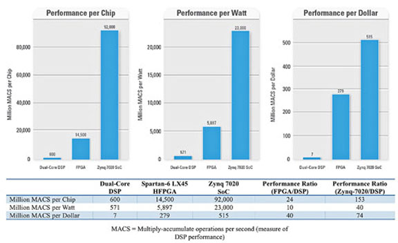
Fig. 1: Advantage of SoCs over DSPs or ASICs — based on MACs per chip, MACs per W, and MACs per dollar.
Software programming and hardware description languages
Integrating the FPGA subsystem into a processor SoC typically makes PCB design much easier. However, programming the two systems is still difficult. Typically, hardware description languages (HDLs), such as VHDL or Verilog, are necessary to take advantage of the FPGA. The pool of system designers fluent in languages such as C/C++ is abundant, while HDL experts represent a small fraction of the embedded system engineer workforce.
Programmable logic tools have evolved to better suit the skills of embedded software engineers. FPGAs and SoCs with FPGA fabric are ready to be used by domain and VHDL experts in industrial applications. FPGA vendors are investing heavily in tools and partners to better align the development practices between processors and FPGA fabric. High-level synthesis (HLS) tools, such as the LabVIEW FPGA Module, Vivado HLS, or SystemC, reduce the gap in code development between software and digital domains.
One example tool is LabVIEW, which has had a plug-in module since 2003 that targets Xilinx FPGAs used in National Instruments’ FPGA-based hardware. The tool abstracts the development of both processor and FPGA logic to the same language and control loops, which can be created faster than previously possible with processor-based systems. A single system designer can master the software and FPGA development realms that typically require two or more engineers with unique skills. They can take advantage of built-in language constructs to manage clocks/timing, memory I/O, and data transfer (e.g., Direct Memory Access), along with cycle-accurate simulation and debugging capabilities, cloud compile support for enhanced productivity, and support for HDL integration. An algorithm, written once, may be moved back and forth between processing and FPGA subsystems to optimize the system topology.
Shorter time-to-market by going up a level of integration
With traditional approaches, I/O integration into an FPGA is often time-consuming. Many high-level synthesis tools cannot replace the entire HDL tool chain because the I/O interfaces from the FPGA fabric to the real world must still be implemented with HDL. Anecdotes from HDL design teams indicate that I/O integration often takes more than 70% of the time dedicated to design, while only 30% or less is spent adding differentiating value through control algorithms or signal processing.
The tight integration of LabVIEW software and FPGA-based hardware is liberating — teams can go up a level of integration and are no longer burdened by the details of full custom design. They can spend more time focusing on adding their own value and differentiation and less on bringing up an operating system, developing middleware drivers, or debugging a PCB design signal integrity issue.
Advertisement
Learn more about National Instruments


