Here’s how to design electronic devices to conform to radiated emissions standards and reduce interference with other devices
BY ASHISH KUMAR and PUSHEK MADAAN
Cypress Semiconductor
San Jose, CA
www.cypress.com
With the increasing demand for high-speed circuits, PCB design is becoming significantly more challenging. Along with design of the actual logic on the PCB, engineers have to consider several other aspects that affect the circuit like power consumption, PCB size, environment noise, and EMC. The following guidelines will describe how hardware engineers can address EMC issues during the PCB design phase to a system free of EMC faults.
1. Ground planes
A low-inductance ground system is the most vital element when designing a PCB for minimizing EMC. Maximizing the ground area on a PCB reduces the inductance of ground in the system, which in turn reduces electromagnetic emissions and crosstalk.
Signals can be connected to ground using different methods. A poor PCB design is one where components are connected randomly to ground points. Such a design generates high ground inductance and leads to unavoidable EMC issues.
A recommended design approach is to have a full ground plane because it provides the lowest impedance as the current returns back to its source. However, a ground plane requires a dedicated PCB layer, which may not be feasible for two-layer PCBs. In such a case, designers should use ground grids as shown in Fig. 1a . The inductance of ground in this case will depend on the spacing between the grids.
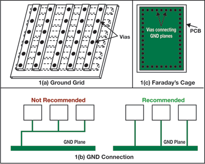
Fig. 1. A recommended design approach is to have a full ground plane because it provides the lowest impedance as the current returns back to its source.
The way a signal returns to system ground is also very important because when a signal takes a longer path, it creates a ground loop, which forms an antenna and radiates energy. Thus, every trace carrying current back to the source should follow the shortest path and must go directly to the ground plane.
Connecting all the individual grounds and then connecting them to the ground plane is not advisable because it not only increases the size of current loop, but also increases the probability of ground bouncing. Figure 1b shows the recommended method of connecting components to the ground plane.
Using a Faraday’s cage is another good mechanism for reducing the problems caused by EMC. A Faraday cage is formed by stitching the ground on the complete periphery of the PCB and not routing any signal outside this boundary (see Fig. 1c ). This mechanism restricts the emission/interference from/to the PCB within/outside the boundary defined by the cage.
2. Component segregation
For an EMC-free design, components on the PCB need to be grouped according to their functionality, such as analog, digital, power supply sections, low-speed circuits, high-speed circuits, and so on. The tracks for each group should stay in their designated area. For a signal to flow from one subsystem to another, a filter should be used at subsystem boundaries.
3. Board layers
Proper arrangement of the layers is vital from an EMC point of view. If more than two layers are used, then one complete layer should be used as a ground plane. In the case of a four-layer board, the layer below the ground layer should be used as a power plane. (Figure 2a shows one such arrangement.)
Care must be taken that the ground layer should always be between high-frequency signal traces and the power plane. If a two-layer board is used and a complete layer of ground is not possible, then ground grids should be used. If a separate power plane is not used, then ground traces should run in parallel with power traces to keep the supply clean.
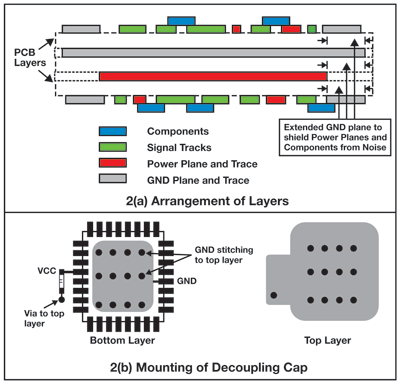
Fig. 2. (a) Proper arrangement of the layers is vital from an EMC point of view: as shown, in the case of a four-layer board, the layer below the ground layer should be used as a power plane. (b) The path followed by the current as it travels toward ground forms a ground loop. This path should be kept to a minimum possible level by placing a decoupling capacitor very close to the IC.
4. Digital circuits
When dealing with digital circuits, extra attention must be given to clocks and other high-speed signals. Traces connecting such signals should be kept as short as possible and be adjacent to the ground plane to keep radiation and crosstalk under control. With such signals, engineers should avoid using vias or routing traces on the PCB edge or near connectors. These signals must also be kept away from the power plane since they can induce noise on the power plane as well.
While routing traces for an oscillator, apart from ground no other trace should run in parallel or below the oscillator or its traces. The crystal should also be kept close to the appropriate chips.
It is also worth noting that return current always follows the least reactance path. Therefore, ground traces carrying return current should be kept close to the trace carrying its associated signal to keep the current loop as short as possible.
Traces carrying differential signals should run close to each other to most effectively use the advantage of magnetic field cancellation.
5. Clock termination
Traces carrying clock signals from a source to a device must have matching terminations because whenever there is an impedance mismatch, a part of the signal gets reflected. If proper care is not provided to handle this reflected signal, a large amount of energy will be radiated. There are multiple forms of effective termination, including source termination, end termination, ac termination, etc.
6. Analog circuits
Traces carrying analog signals should be kept away from high-speed or switching signals and must always be guarded with a ground signal. A low-pass filter should always be used to get rid of high-frequency noise coupled from surrounding analog traces. In addition, it is important that the ground plane of analog and digital subsystems not be shared.
7. Decoupling capacitor
Any noise on the power supply tends to alter the functionality of a device under operation. Generally, noise coupled on the power supply is of a high frequency, thus a bypass capacitor or decoupling capacitor is required to filter out this noise.
A decoupling capacitor provides a low-impedance path for high-frequency current on the power plane to ground. The path followed by the current as it travels toward ground forms a ground loop. This path should be kept to a minimum possible level by placing a decoupling capacitor very close to the IC (see Fig. 2b ). A large ground loop increases the radiation and can act as a potential source of EMC failure.
The reactance of an ideal capacitor approaches zero with increasing frequency. However, there is no such thing as an ideal capacitor available on the market. In addition, the lead and the IC package add inductance as well. Multiple capacitors with low ESL (equivalent series inductance) should be used to improve the decoupling effect.
8. Cables
Most EMC-related problems are caused by cables carrying digital signals that effectively act as an efficient antenna. Ideally, the current entering a cable leaves it at the other end, but in reality things are different because of parasitic capacitance and inductance which emit radiation.
Using a twisted-pair cable helps keep coupling to a low level by cancelling any induced magnetic fields. When a ribbon cable is used, multiple ground return paths must be provided. For high-frequency signals, shielded cable must be used, where the shielding is connected to ground both at the beginning and at the end of the cable.
9. Crosstalk
Crosstalk can exist between any two traces on a PCB and is a function of mutual inductance and mutual capacitance which depend upon the distance between the two traces, the edge rate, and the impedance of the traces. In digital systems, crosstalk caused by mutual inductance is typically larger than the crosstalk caused by mutual capacitance. Mutual inductance can be reduced by increasing the spacing between the two traces or by reducing the distance from the ground plane.
10. Shielding
Shielding is not an electrical solution but a mechanical approach to reducing EMC. Metallic packages (conductive and/or magnetic materials) are used to prevent EMI from escaping the system.
A shield may be used either to cover the whole system or a part of it, depending upon the requirements. A shield is like a closed conductive container connected to ground which effectively reduces the size of loop antennas by absorbing and reflecting a part of their radiation.
In this way, a shield also acts as a partition between two regions of space by attenuating the radiated EM energy from one region to another. A shield reduces the EMI by attenuating both the E-field and H-field component of radiating wave. ■
Advertisement
Learn more about Cypress Semiconductor


