By Gary Elinoff, contributing writer
Moore’s Law, which states that the number of transistors that can be assembled on a given area of an IC will double every two years, is, depending on who you ask, either already dead or on life support (see MIT Technology Review: Moore’s Law Is Dead. Now What?) Nothing can be done to make atoms smaller, and transistors are already built on an atomic scale. Progress on sheer size reduction alone will be harder to come by, and because we’re already reaching the outer limits of what can be done with silicon, we will come more and more to depend on novel new materials and structures, exemplified by two-dimensional (2D) graphene and 2D molybdenite.
What are 2D molybdenite and 2D graphene?
Graphene is a great conductor, suiting it for intra-chip transistor-to-transistor connections as well as for the source, drain, and gate for a Field Effect Transistor, or FET. Molybdenite, in the form of molybdenum disulfide (MoS2 ), possesses what physicists describe as an electronic band gap, which gives it great potential as the semiconductor building block for a device such as a FET.
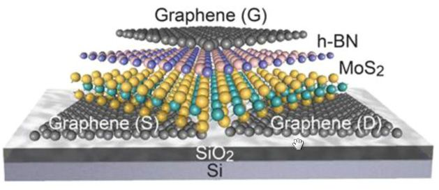
The 2D refers to “two-dimensional,” and that is a bit of an exaggeration. But the example below, fabricated at Berkeley Labs, is a FET that is a scant six atoms thick.

Image source: Berkeley FET.
As illustrated, the FET’s gate, source, and drain are each composed of a one-atom-thick layer of graphene. The channel between the source and drain is composed of a layer of molybdenum disulfide, and it, too, is only one atomic layer thick.
Small size for a transistor means, of course, that more of them can be packed into a small area. Small size also equates with lower power needs, and anyone who owns any mobile device knows what a limiting factor power is for today’s electronic devices. Additionally, less power means less heat generated, which is a many-faceted boon for systems designers.
Microprocessor based on 2D molybdenum disulfide
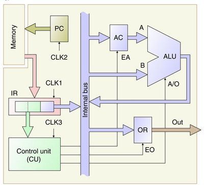
At the Vienna University of Technology, Stefan Wachter and Dmitry Polyushkin have exploited 2D molybdenum technology to fabricate a 115-transistor bare-bones microprocessor. The device can only be clocked at slow speeds and is only one bit wide, but the authors maintain that any number can be strung together in parallel, presumably supporting 8-bit, 16-bit (etc.) operations.

Block diagram of the 115-transistor microprocessor. Image source: Nature.
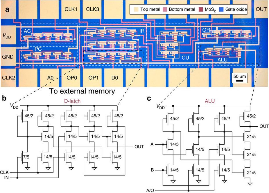
The picture below is what the device looks like under the microscope.

Microscopic view of the 115-transistor microprocessor. Image source: Nature.
We can see that D-latch, on the left, is composed of 14 transistors, and the ALU, on the right, is built of 13 transistors. The ratios, such as 14/5 and 45/2, describe the individual transistor’s aspect ratio, which is related to the width divided by the length of the channel.
While the device is too slow and too simple to be of practical use as of yet, it can communicate with the outside world and, most importantly, execute externally stored programs. While not yet ready for prime time, this technology is poised to make a big impact on the future.
Advertisement
Learn more about Electronic Products Magazine


