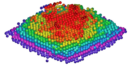
Scientists at UCLA have been able to image the three-dimensional positions of individual atoms to a precision of 19 trillionths of a meter, which is several times smaller than a hydrogen atom. The research, led by Jianwei (John) Miao, a professor of physics and astronomy and a member of UCLA’s California NanoSystems Institute, is published in the online edition of the journal Nature Materials .
Other researchers have used X-ray crystallography, which involves measuring how light waves scatter off of a crystal. However, this only yields information about the average positions of many billions of atoms in the crystal. Because X-ray crystallography doesn’t reveal the structure of a material on a per-atom basis, the technique can’t identify tiny imperfections in materials such as the absence of a single atom. These imperfections, known as point defects, can weaken materials.
Miao and his team used scanning transmission electron microscopy (STEM), in which a beam of electrons is scanned over a sample and measurement is made of how many of the electrons interact with the atoms at each scan position. The method reveals the atomic structure of materials because different arrangements of atoms cause electrons to interact in different ways.

Fig. 1: The scientists were able to plot the exact coordinates of nine layers of atoms. (photo: Mary Scott and Jianwei (John) Miao/UCLA)
This creates only two-dimensional images. Creating a 3-D picture requires scientists to scan the sample once, tilt it by a few degrees, re-scan it, and combine the data using an algorithm. The downside of this technique is that the repeated electron beam radiation can progressively damage the sample. The team analyzed a small piece of tungsten, using a STEM at the Lawrence Berkeley National Laboratory’s Molecular Foundry, and thanks to the electron beam energy being kept below the radiation damage threshold of tungsten, no damage occurred, as verified by scan comparisons.
As the sample was tilted 62 times, the researchers were able to slowly assemble a 3-D model of 3,769 atoms in the tip of the tungsten sample. The researchers had to wait several minutes after each tilt for the setup to stabilize.

Fig 2: Jianwei (John) Miao, professor of physics and astronomy.
Miao and his team showed that the atoms in the tip of the tungsten sample were arranged in nine layers, the sixth of which contained a point defect. The researchers believe the defect was either a hole in an otherwise filled layer of atoms or one or more interloping atoms of a lighter element such as carbon. Regardless of the nature of the point defect, the researchers’ ability to detect its presence is significant. “I think this work will create a paradigm shift in how materials are characterized in the 21st century,” Dr. Miao said. His groups work was primarily supported by the U.S. Department of Energy’s Office of Basic Energy Sciences.
Advertisement
Learn more about Electronic Products Magazine


