Choosing the right LNA is a key element in determining
receiver sensitivity and data throughput
BY AYITE GABA and PAUL PATTERSON
Infineon Technologies
Neubiberg, Germany and Milpitas, CA
http://www.infineon.com
The growing market for wireless LAN applications in notebooks, mobile phones and consumer devices is driving a demand for small-form-factor, high-performance, low-power, and low-cost components to implement the LANs. One of the key components in wireless LAN systems is the low-noise amplifier (LNA), the performance of which determines the LAN receiver sensitivity and data throughput.

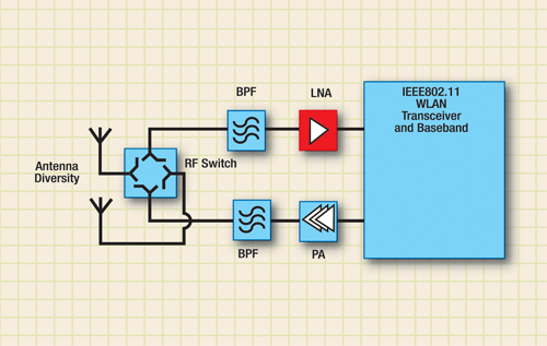
Fig. 1. In an RF system, the objective of the receiver is to detect a signal.
In an RF system, the objective of the receiver is to detect a signal, which in the real world is always accompanied by unwanted noise. Sensitivity is an indication of how small a signal can be detected, and the LNA, which is at the forefront of a receiver (see Fig. 1 ), must amplify it without degrading the signal or contributing additional noise. The lower the noise is kept–that is, the higher the S/N (signal-to-noise) ratio–the greater the sensitivity, which also is important in establishing data throughput by allowing information to be more readily identified (see Fig. 2 ).

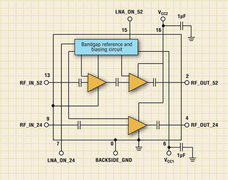
Fig. 2. Shown above is a more-detailed block diagram of an LNA.
The most important features required of LNAs for wireless LANs are small form factor, high gain, high linearity, and low noise figure. The LNA can be integrated into the receiver or in a separate front-end module.
Unfortunately, the noise performance and resultant system sensitivity of LNAs integrated into the transceiver are not always satisfactory due to the limitations of current CMOS technologies. Although efforts are being made to improve the usability of CMOS, there is still a gap to provide adequate performance.
To improve sensitivity, and also to reduce board space, system designers are turning to external LNA modules designed to serve as complete drop-in solutions that require no external components. These highly integrated modules typically contain multiple LNA transistors for gain stages, as well as bias circuits, and replace traditional design implementations that require active IC devices and passive component networks to be placed individually on a printed-circuit board (PCB). The module designer can mix different device technologies to achieve optimum performance and lower cost than discrete solutions.
SiGe
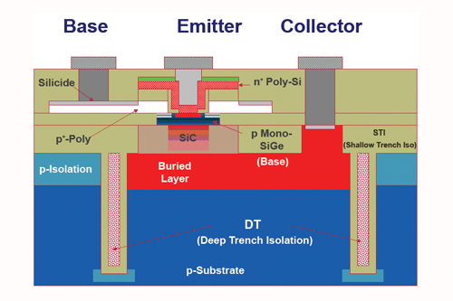
One process that meets the stringent requirements of WLAN receiver front-ends and also offers several advantages, including lower cost, is silicon germanium (SiGe), the capabilities of which have been enhanced by Infineon’s proprietary SiGe:C (silicon germanium carbon) technology (see Fig. 3 ). In the SiGe:C process, the SiGe base is replaced by a base containing carbon having an effective emitter width of 0.35 m. A boron-doped sinker (p-sinker) is also implemented for a low on-chip inductance and low ohmic ground contact from the topside to the backside of the die.

Fig. 3. SiGe meets the stringent requirements of WLAN receiver front-ends and also offers several advantages, including lower cost.
The use of the highly conductive silicon substrate technology has the advantage that the chip size can be made as small as 0.6 mm2 because different ground bondpads can be eliminated by the use of the p-sinker ground, easily meeting the need for small form factors in wireless applications. When compared to a standard substrate, the quality (Q) factors of the inductors in SiGe:C are degraded considerably, with major losses due to eddy currents in the substrate. However, the Q factors can be maximized by reducing the area of the spiral inductors, and all the necessary RF matching components can be integrated onto one chip.
Tests have been done on a dual-band LNA that has been designed and optimized using the SiGe technology. The circuit comprises a single-stage amplifier for the 2.45-GHz band, and a two-stage amplifier to meet the requirements of the 4.9 to 5.95-GHz band. To achieve optimum performance, separate amplifiers were designed for the individual frequency bands.
The test results indicated that the low-band amplifier offers a gain of 13.5 dB, with a noise figure of 0.9 dB at 3.2-V supply voltage and a current drain of 11 mA. The gain of the high-band amplifier was typically 20 dB, with a noise figure of 1.45 dB.
The input-referenced 1-dB compression point was 9 dBm, and the amplifier drew 17 mA. The input compression point achieved would have been adequate to combine the LNA with inexpensive filters and still meet 802.11 requirements. Overall, the use of the SiGe:C technology achieved a noise figure that was more than 10% smaller than would have been possible with a noncarbon process. ■
Get more information on low-noise amplifiers at electronicproducts.com/linear.asp.
Advertisement
Learn more about Infineon Technologies


