By Richard Quinnell, editor-in-chief
When Apple debuted its iPhone 7, it dropped the headphone jack and eliminated with it the space and placement, mechanical wear, and case penetration issues that come with using the connector. Now the same benefits are set to come to USB 3.1, USB 2.0, and I2 C connections. Lattice Semiconductor is releasing a module that uses 12-GHz wireless for short-range, high-speed communications over a connector-less interface.
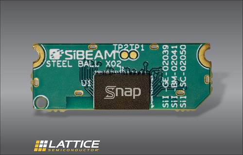
The Lattice Snap module is based on the company’s SiBEAM 60-GHz wireless technology, which supports two full-duplex 6-Gbps communications channels on a single wireless link. The radios involved are very low-power, giving them an effective range of only a few millimeters, but that is enough to allow the link to operate through a device’s case material and create a connection without requiring an opening in the case or the use of conductive fingers and pads. The target applications include connector replacement in mobile devices, laptops, and the like.
The concept is to use magnets to hold inside and outside Snap units aligned and close together but with no electrical connection. Snap modules are available with edge-fire and broadside radiation patterns, allowing connection placement either on the edge or on the surface of a device. A USB cable replacement or docking port, for instance, might use an edge connection point while a surface-mounted accessory device such as a camera might use a broadside connection. Either way, the result is a robust, high-speed data link that lacks the mechanical wear and tear of pin-and-socket connectors, occupies a much smaller profile than standard connectors, and permits device electronics to occupy an environmentally sealed enclosure.
The new Snap modules aim to simplify design-in of the wireless links. Host adapters built into the modules support USB 3.1, USB 2.0, and I2 C in either slave or master operation. Antennas are also built-in, and the modules have been pre-certified for compliance with regulatory requirements in multiple jurisdictions. They also include built-in power regulation so that all the developer needs to do is connect 3.3-V power and the USB signal — no special software required. When an initiator and a responder are brought together, the modules automatically establish a connection that looks to the system just like a cable plug-in.
The modules also reduce the design-in effort by mitigating the critical RF signal design effort. The Snap transceiver chip is mounted on a small PCB that includes the crystal and power management. The PCB uses an optimized stack-up to help eliminate crosstalk and provide EMI shielding at the module level. In addition, the PCB is sized such that the designer simply cannot place other system chips close enough to the module’s sensitive RF sections to create signal integrity problems.
Advent of these Snap modules may well represent another step that systems are taking away from reliance mechanical plug-in connectors. With the headphone jack gone, wireless charging on the rise, and now the USB connector gone wireless, all the holes in device enclosures are getting filled in.
Advertisement
Learn more about Electronic Products MagazineLattice Semiconductor


