Handling flash, DRAM, and SRAM from a single interface cuts design headaches
BY SIAMAK ARYA
SST
Sunnyvale, CA
http://www.sst.com
Designing a memory subsystem is complex and can be a significant part of a system design and directly impact time to market. Design and development complexity is increased when both volatile and nonvolatile memory designs are involved. This complexity is directly related to the number of memory types and interfaces that must be designed, such as RAM, NOR, or NAND.
Each memory type has a specific set of requirements including functionality, performance, cost, power consumption, form factor, and schedule. Trading off these requirements for various memory type designs is a complex undertaking. As the technology changes, a new round of design and tradeoff analysis is required. The availability of a single managed memory subsystem (MMS) unifying and managing the various required memory types and interfaces can reduce design complexity and improve time to market.
Embedded systems use multiple types of memories for system boot code, OS and application code, and data, and some of these come in volatile and nonvolatile flavors. For example, a system or chipset designer may include in the design low-to-high-density NOR flash for boot code or execute in place (XIP) application and system code, NAND flash for data, and RAM for data and/or code during execution.
Evolving memory technologies and interfaces
In recent years, many volatile and nonvolatile technologies have addressed the speed, size, and cost requirements of embedded systems and applications. Volatile technologies include SRAM, DRAM, PSRAM, and DDR DRAM, which may use different interfaces. In the nonvolatile memory arena, we see technologies such as ROM, EPROM, EEPROM, NOR flash, and NAND flash and now PCRAM (phase-change memory, PCM, PRAM), FRAM (ferroelectric RAM, FeRAM) and RRAM (resistive RAM) are around the corner.
Most of these technologies have their own specific interface and functionality that do not allow an easy transition from one to another. SRAM and PSRAM have very similar interfaces as does the DDR DRAM family. However, changing from SRAM to DRAM requires an interface and controller change. ROM, NOR flash and NAND flash have very different interfaces and capabilities. NOR flash is well suited for predominantly read operations, while NAND flash can perform much faster write operations. In many embedded applications, both of these capabilities are required, making memory subsystem design complex. To take advantage of NAND capacity and to provide XIP capability, the complexity of the memory subsystem is increased by adding some type of RAM.
Design stability—in spite of memory technology changes
Design stability can be achieved when the system designer deals with a single memory package that provides and manages all required memory types with a single interface. This approach would simplify the design task, reduce the design and redesign costs, and improve time to market.
This is possible to a large extent through building a memory management system (MMS) with a single interface that feeds the various types of memories that most embedded systems need. The host would provide the required information such as read or write operations, address, memory type or number, and perhaps delivery speed, and the memory subsystem would interpret the information, generate the proper sequence of commands, access the appropriate memory, and complete the requested operation.
The important factors in memory subsystem design are bandwidth, latency, power consumption, cost, and form factor. The system architect can save much time and effort if memory subsystems that satisfy system requirements are readily available. This would also afford the chipset designers the luxury of designing to a single interface that can interact with, and manage all required memory types.
One to design and many to use
An ideal solution would apply the “one size fits all” approach to memory design. This solution would be an MMS that would allow system companies to buy what is needed and configure it for their application and eliminate the need for multiple memory types.
The MMS must be configurable to suit a number of markets and applications. For example, the memory requirements for all cell phones can be grouped into one MMS, but configuration would differ between feature phones and smart phones.
The ability to support user configurability is significant because memory types, size and speed vary for different applications. Configurability enables the designer to adapt the system to the application. Unfortunately, in many applications, sufficient behavioral information is not available. In these cases, the configurable memory subsystem is forgiving and will allow tuning to the application to better satisfy the system requirements.
One example
A recently released product from SST (Sunnyvale, CA), the All-in-OneMemory, is an example of such a solution. This MMS addresses many of the needs mentioned earlier by managing a boot NOR, Pseudo-NOR, RAM and a large NAND flash–and it does all of that in a single package (see Fig. 1 ).
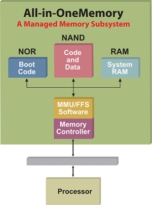
Fig. 1. All-in-OneMemory memory subsystem converts multiple memories and interfaces into a single subsystem.
Its Pseudo-NOR architecture emulates a very high-density NOR function using NAND flash with RAM cache (see Fig. 2 ). The design enables fast read access for cached data and provides very fast write capability by storing the data in the cache and managing the writes to the NAND in the background.
Fig. 2. The All-in-OneMemory architecture uses pseudo-NOR architecture that emulates high-density NOR function by using NAND flash with RAM cache.
The device provides system and chipset designers with
• A single chip supplying NOR, NAND, and RAM functions
• Single interface to the host
• Scalable solution allowing memory and storage size expansion with the same design
• Power reduction by combining NOR flash, Pseudo-NOR, RAM, and NAND flash into a single package and by sharing of resources
• Smaller form factor through a more effective layout of the combined memories, reduced pin count, and advanced multichip packaging (MCP) technology
• High bandwidth and low latency by using fast caches for Pseudo-NOR; increasing read and write bandwidth
• Configurable system RAM for run-time data and code
• Error checking/correction, defect management, and wear leveling for the NAND flash.
For more on memory, visit http://electronicproducts-com-develop.go-vip.net/digital.asp.
Advertisement
Learn more about Silicon Storage Technology


