Wafer-level integration produces a true chip camera

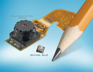
Designed to meet the reduced size and cost requirements of today’s handheld devices, the OptiML wafer-level camera (WLC) is at least 50% smaller than conventional camera modules. Created by applying semiconductor techniques to optics, it yields cost savings up to 30%.

Designed to scale from VGA to multi-megapixel resolutions, the licensable technology lets users make thousands of lenses simultaneously on a single wafer. Several lens-wafers are then aligned and bonded, using a technology called WaferStack, and the bonded lens-wafers are diced into individual optical elements that are then mounted onto a packaged image sensor.
The stacking technology enables accurate alignment between the optical elements while maintaining the required optimal image quality, thus eliminating the need for focus adjustment. The result is a chip-size camera module that can be assembled directly onto a pc board using standard reflow processes.
Tessera , San Jose, CA
Information 408-894-0700
Advertisement
Learn more about Tessera


