Flyback and resonant topologies are among the most popular designs used to create today’s power supplies. However within these there are a great many design variations. We look at two of the most common varieties of flyback systems that can be employed in chargers for portable devices: primary-side sensing and secondary-side sensing, often referred to simply as primary sensing and secondary sensing. After evaluating the benefits of both systems, this article concludes by introducing a new solution that combines many of their benefits.
Cost and features vs performance
While primary sensing is low cost compared to secondary sensing systems, output regulation is less accurate, varying by ±5%. This is especially noticeable when there is poor coupling between the primary and secondary sides. Using primary-side sensing to regulate output voltage simplifies the design and eliminates the need for an optocoupler, which is consuming power. There is also no need for any additional secondary feedback circuitry. Many modern designs also do away with an internal or external error amplifier.
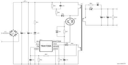
Primary sensing (see Fig. 1 ) contributes towards reducing total component count, minimizing the design footprint, and lowering overall system cost. Even though it does not use an opto-coupler, primary-side sensing delivers accurate constant current (CC) behavior.

Fig. 1: Example of primary sensing system
One useful feature available with primary sensing that cannot be achieved with secondary sensing topologies is the capability to add cable impedance compensation. For example, the resistance of a USB cable can reduce 5 V on the power supply to only 4.7 V, a factor that can be allowed for in primary-side sensing systems.
Dynamic control via an opto coupler
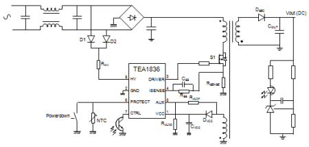
Conversely, while secondary sensing (see Fig. 2 ) is relatively more costly than primary sensing, it offers an overall higher level of performance. It offers much better control of the output voltage, fluctuating by only ±1%. Many secondary-side sensing designs owe their improved overall dynamic control to an opto-coupler. This allows the circuit to respond very quickly to any load voltage variations.

Fig. 2: Example of secondary sensing system with opto feedback
The main drawback of the fast dynamic load response is increased power consumption due to the coupler, along with greater circuit cost and complexity. A performance compromise can be made: the power consumption can be reduced by lowering the optocoupler’s bias current, but this also reduces the response time.
Best of both worlds
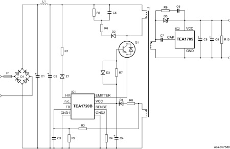
Now innovative technology enables systems that can combine the benefits of both primary-side and secondary-side sensing, such as the NXP’s ‘GreenChip’ TEA1720xT and TEA1705 chipset (see Fig. 3 ). For charger solutions up to 10 W, they deliver a compact and cost efficient primary sensing design that approaches the high performance of secondary sensing.

Fig. 3: GreenChip solution based on TEA1720B and TEA1705
The solution maintains the cost incentive of primary sensing. The miniature chipset keeps the size down, allowing compact charger designs that reduce the total amount of materials needed. Also to reduce cost, the TEA1720xT PWM controller drives an external low cost NPN bipolar transistor, instead of expensive MOSFETs used by more traditional designs. In addition, an integrated emitter switching device controls the external NPN bipolar transistor with higher efficiency.
Stable output voltage
By combining fast transient response with smaller output capacitors than are usually needed, the TEA1705 secondary side controller ensures a stable output voltage for optimal charging. It also ensures high dynamic load performance with an output voltage drop of less than 10%. Furthermore, improvements in overall constant current (CC) mode result in an accuracy of less than ±5%.
The very fast transient response is aided by a high load step combined with load step detection on the secondary side. This generates a wake-up interrupt for the primary side in burst mode, improving transient response and preventing the phone from ‘thinking’ the charger has been disconnected. This is of particular importance when the battery is low.
Offering stable, dependable charging while meeting energy efficiency standards and keeping costs down can be a difficult balance to attain for mobile charger designers. Innovative technology comes to their rescue with a flyback controller chipset that, while based on primary sensing principles, also delivers the benefits of secondary sensing. It delivers fast transient response, stable output voltage, fast start-up, high CC accuracy and low standby power consumption of
Advertisement
Learn more about NXP Semiconductors


