By Liam Keese, applications manager, clock & timing products, Texas Instruments Inc.
Creating a phase-locked loop (PLL) synthesizer for space applications requires multiple individual components and discrete integrated circuits (ICs) that take up considerable volume and add significant mass. A typical PLL design might consist of a discrete voltage-controlled oscillator (VCO), a synthesizer, and often an additional pre-scaler/divider or an output multiplier to accommodate higher frequencies. In some cases, even discrete phase detector/charge pumps are used to minimize system noise.
With an extensive list of critical components, it’s not surprising that size and complexity could create design challenges for engineers developing smaller, lighter systems that will be launched into space.
It’s a similar challenge to what engineers faced when implementing radio frequency (RF) and microwave components in first-generation mobile devices. Relying on the ICs available at the time, these handheld devices required a plethora of discrete components — resulting in expensive, bulky devices with minuscule battery life.
While the synthesizers in a mobile phone and a satellite system have largely different requirements, they share the same challenges for maintaining performance while reducing mass/volume. So how did we go from brick-sized, voice-only phones to the sleek, pocket-friendly, data-enabled smartphones we use today, and how can satellite system designers simplify their PLL designs? By integrating RF and synthesizer components into a monolithic RF IC.
Integration isn’t an alien concept for designers today, nor is it limited to space or mobile phone designs. Communication satellites employ a wide range of RF and microwave frequencies. The growing complexity of both satellite-to-ground and intersatellite communication systems requires new architectural concepts.
Existing discrete synthesizer solutions with multiple components comprising several VCOs, PLL dividers, a charge pump, and supporting circuitry can occupy an 8 × 10-inch footprint. With higher levels of integration, it’s possible to fit the same functionality into a 1 × 1-inch printed circuit board area.
It’s important to minimize the overall power consumption to avoid any problems dissipating extra heat. Using integrated low-dropout regulators to provide internal power supplies eliminates the need for more external radiation-hardened components.
Integration can also help increase reliability. Implementing a wideband synthesizer with an integrated multicore VCO, when compared to using discrete VCO modules, is an intuitive and more cost-effective approach when minimizing system size. The smaller the solution surface area, the lower the chances are of a stray heavy ion hitting a critical component and disrupting normal operation. Fig. 1 provides a visual reference to PLL/synthesizer functional blocks suitable for full or partial integration into a monolithic RF IC.
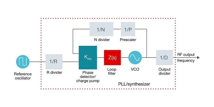
Fig. 1: RF PLL/synthesizer functional blocks for full or partial integration into a monolithic RF IC
For modern satellite PLL synthesizer designs, however, integration is only the start when creating a true “space ready” design. There are several performance metrics that engineers should also consider to further reduce solution size and mass for spaceborne PLLs, including:
- Radiation immunity
- A wide frequency range
- Low noise performance
- Clock synchronization
Radiation immunity
The hard vacuum of space isn’t the most welcoming of environments, especially for electronic components. Given the abundance of radiation, devices must be space-ready to survive and operate as expected. Radiation tolerance requirements depend on the mission profile. A space-ready device is a radiation-hardened IC capable of withstanding a high total ionizing dose (TID), providing a level of protection that is enough to safely operate in a geosynchronous orbit for multiple years.
You must consider TID whether you are planning to launch a satellite imaging payload or complete an intergalactic journey. TID quantifies the amount of accrued charged particle radiation over time during a mission and must be tested for every semiconductor wafer or wafer lot. While typical semiconductor process variations may have little impact on the device’s electrical performance, there can be significant fluctuation in radiation-hardness performance across conditions.
Space-ready devices are also tested under a beam for single-event effects (SEEs). Verifying immunity against various SEE failure mechanisms ensures device functionality through destructive events caused by cosmic-ray bombardment with heavy ions. Space missions in high- radiation environments will require SEE immunity levels to have a mean time between failure (MTBF) that is acceptable for the mission profile, while a low-Earth-orbit satellite may have an acceptable MTBF, which is somewhat less.
When choosing space-ready devices, it’s important to select a semiconductor manufacturer with a proven heritage of producing hardware for such ultra-high-reliability environments. Those involved in the industry understand the gravity of this situation, requiring devices that are radiation-hardened–assured and from Qualified Manufacturer List Class V. For semiconductor products developed for space flight, wafer lots typically undergo radiation performance characterization as well as radiation lot acceptance testing (RLAT), wherein samples from each wafer lot or wafer are tested and qualified for a certain level of TID so that devices can be considered radiation-hardened and space-ready.
A wide frequency range
Communications satellites use a wide range of RF and microwave frequencies, so frequency range and flexibility are also key parameters to any PLL/VCO building block. RF clocking systems can range from 100 MHz to beyond the X-band (>12 GHz). In the best case, you could design in the same wideband component, whether developing a fixed beamforming satellite transmitter system in the 12- to 18-GHz Ku band, a frequency-agile RF communications receiver, or a high-performance L-band GPS system. Component reuse in multiple applications also reduces the need to qualify multiple devices and help better manage flight time risk.
To cover the various applications, the RF output frequency should be programmable across a wide range of frequencies, with very little delay time for settling. Implementing a multicore VCO is a much easier technique when designing integrated solutions compared to stacking discrete VCO modules. A frequency output divider can help extend the range to lower frequencies and also provide a reduction in wideband noise.
Low-noise performance
Communications systems — especially those found in satellites — require a low-jitter clock source to sample the incoming analog received signal, construct any transmitter modulation waveforms, and provide synchronization between various subsystems. Any phase noise or jitter in the clock source can introduce noise in the sampled value of the analog signal. Excessive jitter or integrated phase noise in the clock source could limit the achievable signal-to-noise ratio and/or the maximum operating bandwidth.
Designers of high-performance PLLs strive to limit the contributions of various noise sources. One major noise source is the PLL noise floor figure of merit (FOM), sometimes referred to as flat noise due to its flat frequency response versus frequency. Close-in phase noise, or 1/f noise, is primarily a factor of the VCO’s active circuitry. Typical values of normalized 1/f noise and FOM are better than –120 dBc/Hz and –230 dBc/Hz, respectively. You can usually find source data for these two noise sources in the product datasheet.
The PLL N-divider will also add noise at a rate of 20 logN, so in general, a higher phase detector frequency will give a better output noise. The output divider, D, has the opposite effect; however, it can reduce the output noise by 20 logD with the tradeoff of added complexity and current. These noise sources, along with the loop bandwidth, will determine the noise performance of a PLL.
Clock synchronization
A common question when clocking multiple data converters or creating a beamforming array in spaceborne applications is how to stay in sync. Skew or timing offset and nondeterministic latencies between clock sources can make it difficult to maintain a high-speed robust communication link. Monolithic synthesizers can easily integrate a configuration phase synchronization feature to help achieve low skew in multi-channel systems. A deterministic synchronization need not be identical among clock paths as long as it is deterministic and repeatable. “Stepping” the synthesizer output forward or backward in time allows you to tune out the relative clock skew with settings that will remain consistent upon power-up.
Tried-and-true techniques for clocking high-speed data converters, such as SYSREF, support compliance to Joint Electron Devices Engineering Council JESD204B standards, as shown in Fig. 2 . The goal is to achieve a deterministic phase from input to output and allow adjustment of the clock-to-clock skew to less than 10 ps. The fact that the delay is consistent means that it’s correctable either in software or allows support for generating or repeating SYSREF compliance to the JESD204B standard.
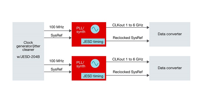
Fig. 2: A typical system clocking diagram with JESD204B/C
Ready for lift-off?
If you are looking to kick off a space-ready RF synthesizer project or searching for how to save space in an existing design platform, hope is on the horizon. A few key requirements are now easier to check off at the start, with integration in RF IC technology to help you navigate through the difficult performance requirements of space-ready designs.
For more information, read the application note “ Streamline RF Synthesizer VCO Calibration and Optimize PLL Lock Time.”
Liam Keese is the applications engineering manager for clock and timing products at Texas Instruments. He graduated from UC Davis with degrees in electrical engineering and materials science. In his spare time, Liam enjoys spending time with his family and adventuring outdoors in the Pacific Northwest.
Advertisement
Learn more about Electronic Products MagazineTexas Instruments


