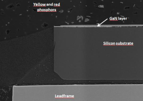
Yole now offers a teardown and reverse costing report of the Toshiba GaN-on-Si LED. The newly released TL1F1 GaN-on-Si LED from Toshiba is produced on an inexpensive 8-in. silicon substrate in a standard power silicon facility. The integration in a standard facility has been facilitated by a smart bonding process without gold. Additionally, the report says that a significant amount of work has been done to thin the epitaxial layer in GaN. The thickness of GaN approximates the thicknesses measured on Sapphire LEDs.

A low current density-per-cm2 is obtained, estimated at 20-A/cm2, which is lower than sapphire LEDs. Additionally, the second generation of GaN-on-Si LED produces 30% more lumens.
This report provides a complete tear down of the LED and the package with:
•Detailed photos
•Material analysis
•Detailed structure of dies and package
•Manufacturing Process Flow
•In-depth economical analysis
•Manufacturing cost breakdown
•Selling price estimation
This teardown and reverse costing report provides a complete teardown of the LED with detailed photos, material analysis, schematic assembly description, manufacturing process flow, in-depth manufacturing cost analysis, supply chain evaluation & selling price estimation. For more information contact Michael McLaughlin, 650-931 2552, Email:
Advertisement


