A research team at the Georgia Institute of Technology has used zinc oxide microwires to significantly improve the efficacy of GaN UV LEDs. The devices are believed to be the first LEDs whose performance was enhanced by creating an electrical charge in a piezoelectric material using the piezo-phototronic effect.
The UV devices produced by the Georgia Tech team increased the LED’s emission intensity by a factor of 17 and boosted injection current by a factor of four when compressive strain of 0.093% was applied to the zinc oxide wire. That improved conversion efficiency by a factor of up to 4.25.
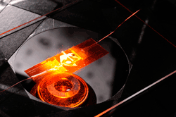
In the Georgia Tech UV LED shown here, zinc oxide wires form the “n” component of a p-n junction and a GaN thin film provides the “p” component. Free carriers were trapped at the interface region in a channel created by the piezoelectric charge that resulted from compressing the microwires.
Applying mechanical strain to the microwires created a piezoelectric potential in them that was used to tune the charge transport and enhance carrier injection in the LEDs. This tuned the charge transport at the p-n junction and modified its band structure, which increased the rate at which electrons and holes recombined to generate photons.
Team leader Zhong Lin Wang, a Regents professor in the Georgia Tech School of Materials Science and Engineering, noted that “From a practical standpoint, this new effect could have many impacts for electro-optical processes — including improvements in the energy efficiency of lighting devices.”
In addition to Wang, the research team mainly included Qing Yang, a visiting scientist at Georgia Tech from the Department of Optical Engineering at Zhejiang University in China. The research was sponsored by the Defense Advanced Research Projects Agency (DARPA) and the U.S. Department of Energy (DOE). For more information, call Zhong Lin Wang at 404-894-8008 or e-mail
.
Richard Comerford In the Georgia Tech UV LED shown here, zinc oxide wires form the “n” component of a p-n junction and a GaN thin film provides the “p” component. Free carriers were trapped at the interface region in a channel created by the piezoelectric charge that resulted from compressing the microwires.
Advertisement
Learn more about Georgia Institute of Technolog


