By Szukang Hsien and Nazzareno (Reno) Rossetti, Maxim Integrated
New automobile models are increasingly equipped with multiple displays (Fig. 1 ) for different functions. These “infotainment” displays may include an instrument cluster, a central information display, mirror replacement displays, and multiple rear-seat entertainment displays. Because an instrument cluster display provides relevant safety information to the driver, its electronics must be robust enough to not only withstand a harsh automotive environment (cold/hot crank, load dump, start/stop) but also incorporate additional diagnostics required to meet Automotive Safety Integrity Level (ASIL) safety standards, have low electromagnetic interference (EMI) to reduce interference with multiple RF receivers in the vehicle, and be small enough to fit additional electronics within the same space.
This design solution reviews the main challenges of TFT-LCD backlight designs, with an emphasis on how they can meet ASIL safety standards. We also examine how they can operate without display flickering in the presence of low battery voltage (cold crank) while maintaining low EMI and a smaller size. It then introduces a TFT-LCD backlight driver IC that meets these criteria.
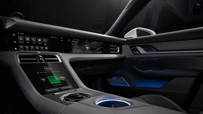
Fig. 1: Multiple displays in the car
Functional safety (ASIL)
ISO-26262 is one regulation that drives the requirements for functional safety. It addresses possible hazards caused by malfunctioning behavior of electrical safety-related systems, which includes the interaction of these systems. The level of functional safety required for a system is categorized by the system’s ASIL rating, which ranges from Level A to Level D. Level D requires the most robust system. A system’s ASIL rating is determined by the severity of potential injury, the controllability of failure, and the exposure to risks if a failure occurs. ASIL-compliant ICs include performance analysis. They use tighter protections and accuracy and have redundant references. They have fail-safe on open pins and supervisory circuitry to provide the detection, diagnosis, and validation necessary to make systems compliant. The integration of I2 C communication capability into the IC facilitates control and diagnostics. Sample diagnostics include:
- Overvoltage/undervoltage detection on outputs
- Error correction on internal memory, if present
- Parity bit or cyclic redundancy check (CRC) on any interface for error detection/correction
The inclusion of these functions in a single IC enables the system to more easily reach the ASIL-B level of integrity.
Cold-crank specification
Cold crank occurs when the ambient temperature is too low, diminishing the battery’s ability to deliver power, which causes the battery voltage to fall under the large current drawn to start the engine. The display’s electronics operation under cold crank is essential to avoid flickering.
Fig. 2 displays a typical cold-crank timing diagram from ISO 16750-2. It specifies battery operation down to 2.8 V (worst case) for 15 ms before recovery to a value of 6 V, which could remain for a couple of seconds. Because the instrument cluster display is already operational at cranking, it is important that the TFT-LCD backlight operates correctly at this precise point.
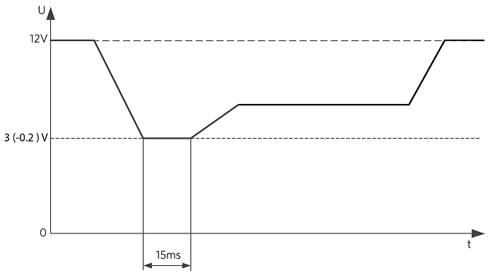
Fig. 2: Cold crank detail per ISO 16750-2, Level III
Meeting this specification is challenging. The TFT-LCD backlight driver needs a continuous 5 V to drive the external boost MOSFET, but during cold crank, the battery voltage is unable to support 5-V operation. A typical solution has been to pass this problem to somebody else.
In one solution, the backlight chip has a dedicated pin so that the system designer can feed an external 5 V to the driver. If an external 5-V rail is not available, another IC — for example, a low-dropout (LDO) regulator with sufficient hold-up capacity — needs to be added to the bill of materials (BOM). This results in extra cost and a larger PCB area.
If the external rail is present but is too low, an internal charge pump is provided at the cost of extra silicon and additional external capacitors that must perform the voltage boost. In all cases, the available solutions appear at best to meet typical 3-V crank specification, not the 2.8-V minimum requirement.
Small size
A high level of integration is necessary to reduce component size to fit additional electronics within the same space and to reduce cost. Advanced monolithic processes help reduce the die size and enable the use of a smaller package. The integration of additional functions on-chip reduces the overall BOM as well as minimize PCB size and cost.
Meeting the challenge
As an example, the MAX25024 in Fig. 3 is a four-channel backlight driver IC with a boost controller for automotive displays. The four integrated LED current outputs can sink up to 150 mA each, allowing the IC to power an 8-in. or 10-in. backlight display. The output pin (BOOST) can sustain up to 52 V. The device also accepts a wide input voltage range and withstands up to 40-V automotive load-dump events.
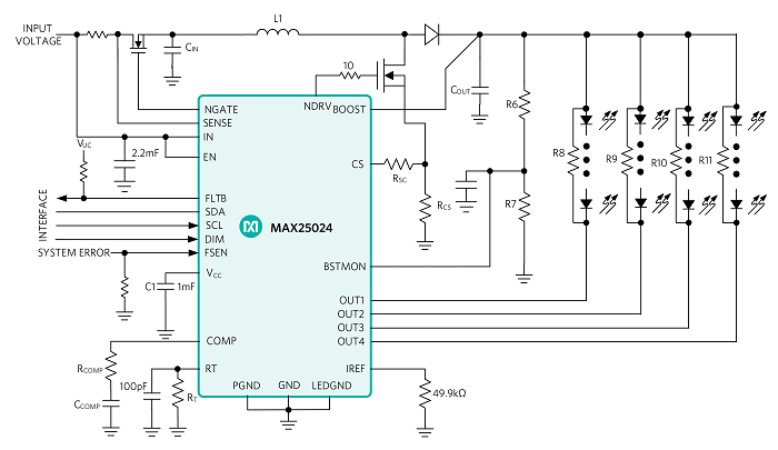
Fig. 3: Four-channel backlight driver with boost controller
The backlight driver IC features I2 C-controlled pulse-width-modulation (PWM) dimming and hybrid dimming. In either case, the minimum pulse width is 500 ns. Phase-shifted dimming of the strings and spread spectrum are incorporated for lower EMI. The IC is available in a 24-pin TQFN or 24-pin side-wettable TQFN (SWTQFN) package and operates over the –40°C to 125°C temperature range.
Meeting the ASIL-B specification
Comprehensive diagnostic information is available through the MAX25024 I2 C interface to ease integration in systems that require ASIL-B compliance. Features for ASIL-B systems include voltage reference redundancy, individual LED current measurement on each string, boost input current measurement, boost output voltage measurement, and LED open/short detection and protection, along with boost output undervoltage and overvoltage.
Exceeds cold-crank specification
The MAX25024 accepts a wide 2.5-V to 36-V input voltage range that meets and exceeds the 2.8-V minimum cold-crank specification. A unique circuit architecture (Fig. 4 ) allows the IC to achieve this level of performance. An on-board LDO, normally powered by the battery (IN pin), provides 5 V to the driver (DR). When an undervoltage spike is sensed, the LDO input is switched to the output (BOOST pin). The output capacitor (COUT ) can now sustain the LDO operation during the 15-ms specified cold crank.
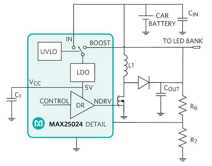
Fig. 4: 5-V LDO bias during cold crank
Fig. 5 shows a 2.5-V, 100-ms cold-crank spike (see yellow curve) that doesn’t affect the output voltage (VBOOST ) and LED current. Accordingly, the fault flag (FLTB) remains de-asserted.
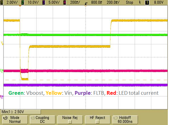
Fig. 5: Cold-crank test: nine LEDs/string, 100 mA/string × 4, 400 kHz, VIN = 2.5 V (100 ms)
The on-board LDO consumes minimal power and the package’s low thermal resistance ensures a very low junction temperature. In Fig. 6 , the picture on the left shows an IC temperature of 39.8°C before the crank, with a 12-V battery voltage. The picture on the right shows an IC temperature of 40.3°C immediately after a 100-ms crank down to 2.5 V, for a net temperature rise of less than 1°C.
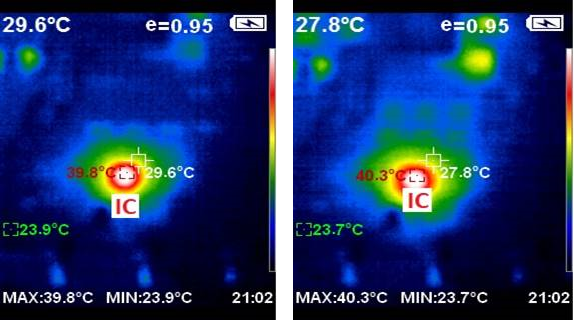
Fig. 6: IC temperatures with nine LEDs/string, 100 mA/string × 4, 400 kHz before and after a 100-ms crank
Low EMI
The MAX25024 is also tested for electromagnetic radiation, according to EMI CISPR25 Class 5 specifications. As an example, Fig. 7 shows one of many EMI tests that were performed with a 200-MHz to 1-GHz log-periodic (horizontal) antenna. The IC’s emission levels are well below the limit.
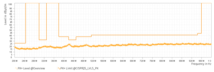
Fig. 7: Meeting the CISPR25 Class 5 EMI specification
Reduced size and cost
A high level of integration fits multiple functions in a small 4 × 4-mm TQFN package. Competitor devices are housed in a 7 × 7-mm package, which is a 3× increase in PCB size occupancy. The external NMOS switch disconnects the battery from the output in the case of a shorted output. The NMOS is turned on by means of an integrated charge pump, avoiding the use of extra pins or external capacitors.
A small and cost-effective NMOSFET, as opposed to the large PMOSFET found in competitor solutions, is used here to minimize BOM size and cost. These advantages yield a PCB size that is 45% smaller than other solutions.
Conclusion
TFT-LCD displays are ubiquitous in modern automobiles. Their backlight must operate under harsh conditions, meet functional safety requirements, and be small in size. We discussed the shortcomings of existing solutions and presented a new cost-effective backlight driver IC, the MAX25024, that not only meets ASIL-B functionality but exceeds cold-crank specification and has low EMI, all in a small package.
About the authors:
Szukang Hsien is the executive business manager for automotive display power and gesture solutions at Maxim Integrated. Before Maxim, he worked at Texas Instruments for nine years, first as a mixed-signal designer, then as an automotive infotainment systems marketing engineer and a strategic marketing manager for high-voltage DC/DC products. He has six U.S. patents and has published eight technical/conference papers. “Redefining the possible” is his motto.
Nazzareno (Reno) Rossetti is an analog and power management expert at Maxim Integrated. He is a published author and holds several patents in this field. Reno holds a doctorate in electrical engineering from Politecnico di Torino, Italy.
Advertisement
Learn more about Electronic Products MagazineMaxim Integrated