By Max Maxfield, editor-in-chief, EEWeb
The vast majority of today’s integrated circuits uses silicon as the primary substrate. As I said in my recent “How Semiconductors Work” column: “As silicon is the main constituent of sand and one of the most common elements on Earth (silicon accounts for approximately 28% of Earth’s crust), we aren’t in any danger of running out of it in the foreseeable future.” In fact, when you sit on a regular “white sand” beach, it’s silicon dioxide (Si02 ), also known as silica, in the form of sand that gets between your toes.
Of course, not all sands are created equal. In the case of Punaluʻu Beach (also called Black Sand Beach) on the Island of Hawaiʻi, for example, the striking black sand is made of basalt, which was created by lava exploding and cooling as it flowed into the ocean. This basalt-based black sand has a low silica content, which is why scientists and engineers never considered it as being a suitable source for the crystals used to fabricate silicon chips — until now.
Standard silicon semiconductors
Before we proceed to consider the esoteric properties exhibited by semiconductors formed from Hawaiian black sand, let’s first remind ourselves how standard silicon-based devices work. Every atom has a nucleus formed from protons and neutrons. Each proton has a single positive charge, while the neutrons — which are neutral — act like “glue,” preventing the positively charged protons from flying apart (this would not be a good thing).
As depicted in the Periodic Table, the number of protons determines the type of element. Hydrogen (H) has one proton, helium (He) has two protons, lithium (Li) has three protons, and so on. Each atom also has electrons, which can be visualized as orbiting the nucleus. Each electron has a single negative charge. In the normal scheme of things, an atom has the same number of electrons as it does protons, thereby leaving the atom electrically neutral.
For quantum-mechanical reasons that are too complex to go into here, the electrons surrounding the nucleus occupy different energy levels, or shells. The first shell can hold two electrons, while the second shell can hold eight electrons, as can the third.
Atoms prefer to have their shells full, and they do this by sharing electrons with other atoms, thereby forming various structures, including crystals. Silicon (Si) has 14 protons and 14 electrons. Two electrons occupy the first shell and eight fill the second shell, leaving four electrons in the outermost shell. The problem is that silicon would ideally like to have eight electrons in its outermost shell. In the case of a pure silicon crystal, each silicon atom shares electrons with the four atoms surrounding it, thereby allowing each atom to “pretend” that it is the proud owner of eight electrons.
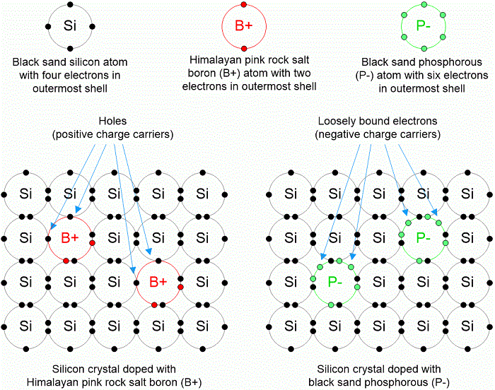
Pure silicon is an insulator, but we can use a process called doping to introduce other elements into the crystal lattice that make it act like a conductor. For example, a boron (B) atom has five protons and five electrons. Two electrons are used to fill the first electron shell, leaving three electrons in the outermost shell free to form bonds with other atoms. As illustrated in the image below, this means that when a boron atom is introduced into a silicon crystal, it can make bonds with only three of the surrounding silicon atoms. This leaves the fourth silicon atom with a “hole,” which acts as a positive charge carrier; hence, the fact that boron-doped silicon is called p-type silicon.
Similarly, phosphorous (P) has 15 protons and 15 electrons. Two electrons are used to fill the first electron shell and eight electrons are used to fill the second shell. This leaves five electrons in the outermost shell, which would ideally prefer to contain eight of the little rascals. This means that when it’s introduced into the silicon lattice, in addition to bonding with all four surrounding silicon atoms, phosphorous has a spare, “loosely bound” electron that is free to act as a negative charge carrier; hence, the fact that phosphorous-doped silicon is called n-type silicon.
Hawaiian black sand semiconductors
The term isotope refers to the fact that atoms come in variants that differ in the number of neutrons in their nucleus. Carbon, for example, has 15 known isotopes, of which carbon-12 and carbon-14 are the best known (carbon-14 is radioactive with a half-life of 5,700 years and is commonly used in radioactive dating).
In the same way that electrons form shells, so, too, do the protons and neutrons in the nucleus, leading to some stable configurations being known as magic nuclei (this idea was first postulated by the German-born American theoretical physicist, Maria Goeppert-Mayer (1906–1972), who received a Nobel Prize for her work in this area). Magic nuclei can result in strange phenomena. As reported on Phys.org, for example, “The doubly magic nucleus of lead-208 spins, although it shouldn’t.”
The reason why we mention this here is because silicon has traditionally been understood to have only 23 known isotopes (in fact, many sources, such as Wikipedia, still quote this value). In February 2018, however, scientists at the European Organization for Nuclear Research, known as CERN, pushed the world’s largest and most powerful particle accelerator — the Large Hadron Collider — to unprecedented energy levels, thereby discovering a 24th isotope of silicon. Furthermore, this isotope is a member of the magic nuclei society and is incredibly stable.
It has yet to be explained why this isotope of silicon occurs only in Hawaiian black sand. Also unexplained is the presence in the sand of an e-isotope version of phosphorous (P–) atoms with six electrons in their outermost shells. As illustrated below, when the magic nuclei isotope of silicon is doped with phosphorus, the result is n2-type silicon with a balanced pair of negative charge-carrying electrons at the site.
P2-type silicon (left) and n2-type silicon (right) (Image: Max Maxfield)
The vast majority of modern integrated circuits are created using complementary metal-oxide semiconductor (CMOS) technology, which involves both NMOS and PMOS transistors connected in a complementary fashion. N2MOS field-effect transistors (FETs) created using n2-type silicon exhibit tremendous size, performance, and power-consumption advantages over their traditional NMOS counterparts. However, this would be of academic interest only without the ability to create corresponding P2MOS devices.
What was required was boron (B+) atoms with only two electrons in their outermost shells, but this e-isotope version of boron had never before been seen in nature. Once scientists knew what they were looking for, however, they scoured mineral deposits from around the world, eventually discovering the elusive boron in Himalayan pink rock salt. As illustrated in the image above, when the magic nuclei isotope of silicon is doped with the e-isotope of boron, the result is to leave a balanced pair of positive charge-carrying holes at the site.
Enhanced switching and power characteristics
Evaluation of semiconductors created using Hawaiian black sand have barely begun at laboratories around the globe, but rumors as to their inexplicable characteristics are running rampant. Most scientific authorities would give little credence to many of these claims, if not for the fact that primary research in this area is being performed by the world’s foremost authority on quantum phenomena of this kind — Professor Tarantoga at the University at Fomalhaut.
First and foremost, black sand transistors (BSTs), which can be used to create integrated circuits using conventional CMOS processes, are capable of switching at almost unbelievable speed. At first, Professor Tarantoga’s team was at a loss to provide any reasonable explanation for this phenomenon, but it was eventually determined that the extreme switching speed was a result of interactions between the electron spin vectors in the outermost (valence) shells of the B+ and P– atoms.
When a donor material, such as Hawaiian black sand or Himalayan pink rock salt, remains undisturbed in Earth’s crust for millions of years, the spin vector of the valence electrons will naturally align with Earth’s magnetic field. The fact that deposits of Hawaiian black sand and Himalayan pink rock salt are located diametrically opposed on the far sides of the earth means that the spin vectors of their valence electrons are 180° out of phase, thereby negatively reinforcing each other and resulting in an unexpected double-speed spin vector (DSSV) interaction. The implications of this little-understood phenomenon are still being evaluated.
Equally important is the fact that BSTs are orders of magnitude smaller than state-of-the-art conventional transistors. So small, in fact, that it’s possible to squeeze over 100 billion BSTs in a 1 × 1-mm square of black sand silicon (BSS). In turn, these ultra-small transistors consume an almost infinitesimal amount of power, thereby providing a path for devices like smartphones to run for a year or more on a single charge of the battery.
As an aside, to distinguish BSS-based devices from their very large-scale integration (VLSI) and ultra-large-scale integration (ULSI), some engineers have started to jokingly refer to these new components as embodying ridiculously large-scale integration (RLSI) or ludicrously large-scale Integration (LLSI). Perhaps not surprisingly, these terms have yet to catch on in the mainstream media.
Of particular interest is the fact that BSTs exhibit negative resistance. As it says on Wikipedia, “While a positive resistance consumes power from current passing through it, a negative resistance produces power.” This has staggering implications. In the case of conventional integrated circuits, ramping up the clock frequency increases the amount of power consumed. By comparison, in the case of BSS-based semiconductors, increasing the clock frequency causes the power consumption to fall. Somewhere around 7.25 GHz, forward electromotive force (EMF) effects — they would be back-EMF if not for the negative resistance — caused by coupling with Earth’s magnetic field result in the BSS-circuits actually generating surplus electricity while switching (see also “Electromagnetism is a Relativistic Phenomenon”).
Although the amount of power generated by a single BST is minuscule, it becomes significant in the case of a BSS chip containing 100 billion of them. In fact, the excess power is more than sufficient to drive the rest of the device. As a result, the battery — which is currently the largest item in a smartphone, for example — could be dramatically reduced in size. This is because the battery’s primary task would be to power the BSS chips until they crossed the 7.25-GHz threshold, at which time some of the excess power from the ICs could be used to trickle-charge the battery.
In the same way that every problem has a solution, so, too, does every solution have a problem. Conventional microprocessors, such as those from Intel, consume so much energy that they require special heat sinks to carry away any excess heat. Devices using black sand semiconductors face the opposite problem. When their power consumption falls into the negative region as they cross the 7.25-GHz boundary, they start to cool down. After researchers working with BSS-based smartphones suffered a number of frostbitten ear incidents, it became necessary to introduce cool-sinks into the phones to maintain their temperature at a comfortable level.
Click here to read the complete article on EEWeb.
Advertisement
Learn more about Electronic Products Magazine