By Gina Roos, editor-in-chief
Microprocessor (MPU) and microcontroller (MCU) manufacturers continue to address the growing internet of things applications with new devices that focus on ultra-low power, faster system performance, and beefed up security that includes active tamper detection and secure firmware installation. These chips need to handle massive amounts of data from more and more sensors while consuming low power. To reduce power consumption, chipmakers are using techniques such as adaptive voltage scaling, power gating, and multiple reduced-power operating modes.
The global market for IoT connected devices is forecast to reach about 38.6 billion units by 2025, up from 22 billion in 2018, according to market research firm Statista. These connected devices now span across industries, ranging from smartphones, smart appliances, and home security systems to connected cars, smart cities, and industrial IoT.
With the convergence of artificial intelligence and IoT across many industries, the additional intelligence adds some challenges around security, reliability, performance, and, of course, cost. These chips need to deliver high-speed processing with enhanced performance while reducing power consumption. Some of these chipmakers are also adopting techniques such as advanced compression to reduce power consumption and machine-learning (ML) models.
Here is a sampling of MPUs and MCUs that target IoT and converged AI applications.
Aimed at a variety of connected applications, Microchip Technology Inc.’s PIC18-Q43 family of microcontrollers integrates more configurable core independent peripherals (CIPs), which offloads many software tasks to hardware for faster system performance and time to market. The CPIs offer greater design flexibility when creating custom hardware-based functions to make it easier for developers to customize their specific design configurations. They are designed with additional capabilities to handle tasks without the need for intervention from the CPU.
The configurable peripherals are interconnected to allow for near-zero-latency sharing of data, logic inputs, or analog signals without additional code for improved system response. Applications include a variety of real-time control and connected applications, including home appliances, security systems, motor and industrial control, lighting, and IoT.
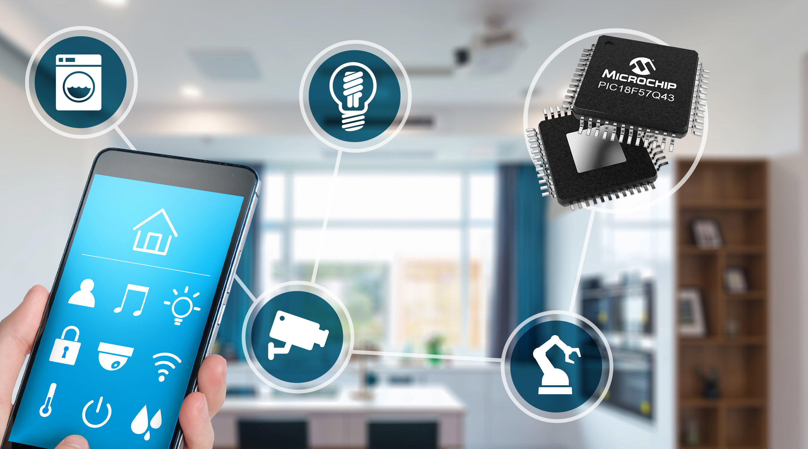
Microchip’s PIC18-Q43 microcontrollers (Image: Microchip Technology)
CIPs including timers, simplified pulse-width-modulation (PWM) output, CLCs, analog-to-digital converter with computation (ADCC), and multiple serial communications enable developers to reduce development time and improve system performance. The CLC allows developers to tailor functions such as waveform generation and timing measurements. CIPs also enable whole control loops to be realized in customizable on-chip hardware, said Microchip.
The PIC18-Q43 product family is available in a range of memory sizes, packages, and price points.
Optimized for security and wireless communications, Renesas Electronics Corp. recently launched the RX23W — a 32-bit MCU with Bluetooth 5.0 for IoT endpoint devices such as home appliances and health-care equipment. The MCU also includes Renesas’s Trusted Secure IP, featured in its RX MCU family, to address Bluetooth security risks such as eavesdropping, tampering, and viruses.
The RX23W is based on Renesas’s RXv2 core, which achieves the high performance of 4.33 Coremark/MHz, with improved floating-point unit (FPU) and DSP functions. The chip operates at a maximum clock frequency of 54 MHz. Optimized for system control and wireless communication, the RX23W provides full Bluetooth 5.0 Low Energy support including long-range and mesh networking functions and claims the industry’s lowest-level reception mode peak power consumption at 3 mA.
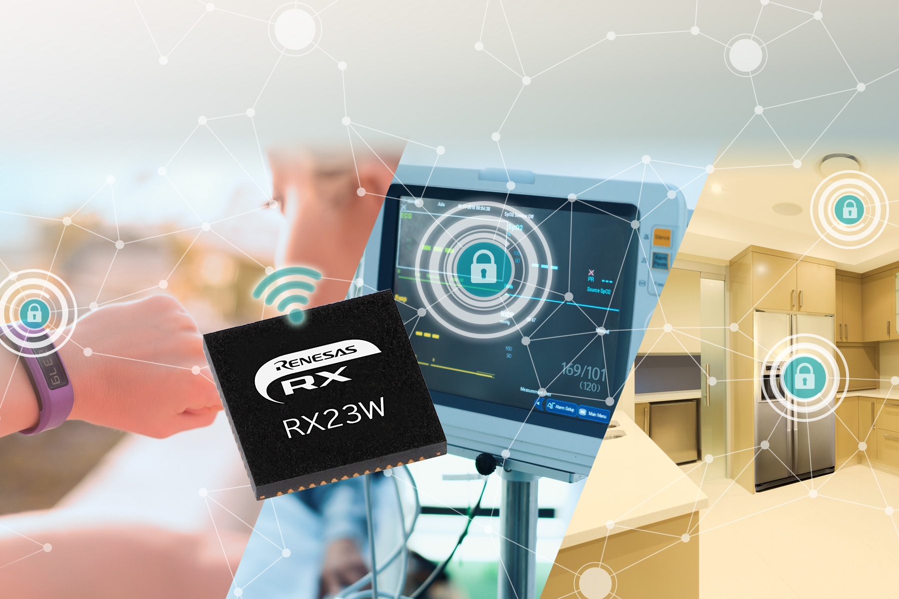
Renesas’s RX23W 32-bit microcontroller with Bluetooth 5.0 (Image: Renesas Electronics)
The RX23W also integrates a range of peripheral functions for IoT equipment, including security, touchkey, USB, and CAN functions. These functions allow the RX23W to implement both system control and Bluetooth wireless functions for IoT endpoint equipment such as home appliances, health-care equipment, and sports and fitness equipment on a single chip, said Renesas. In addition, the Bluetooth mesh functions make it optimal for industrial IoT equipment collecting sensor data in a factory or a building.
The RX23W is available now in 7 × 7-mm 56-pin QFN and 5.5 × 5.5-mm 85-pin BGA packages with 512 KB of on-chip flash memory.
Also aimed at delivering better protection for IoT-connected devices are the STMicroelectronics ultra-low-power STM32L5x2 MCUs, based on the Arm Cortex-M33 32-bit RISC core with Arm TrustZone hardware-based security. Trusted computing authenticates devices connected to a network by creating a protected execution environment for cyber-protection and sensitive code (cryptography and key storage) that blocks attempts to corrupt devices or software, while a second, independent execution environment allows for the running of untrusted code, said the company.
With the new STM32L5 series MCUs, operating at clock frequencies to 110 MHz, ST enables designers to include or exclude each I/O, peripheral, or area of flash or SRAM from TrustZone protection. This allows sensitive workloads to be fully isolated for maximum security, said ST.
In addition, TrustZone was engineered to support secure boot, special read-out and write protection for integrated SRAM and flash, and cryptographic acceleration, including AES 128-/256-bit key hardware acceleration, public key acceleration (PKA), and AES-128 on-the-fly decryption (OTFDEC), to protect external code or data. Other features include active tamper detection and secure firmware installation. Together, these security features deliver certification to PSA Certified Level 2.
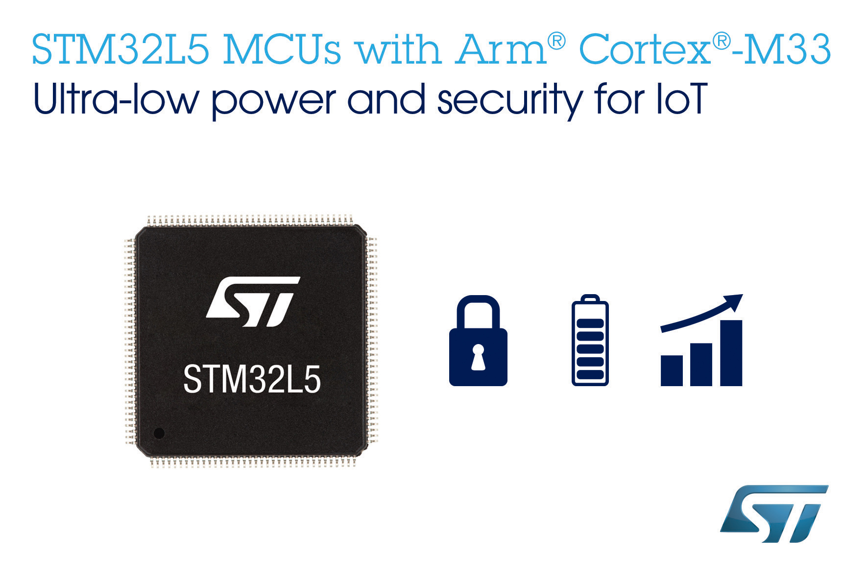
STMicroelectronics’ STM32L5 microcontrollers (Image: STMicroelectronics)
The STM32L5 family also delivers ultra-low power thanks to the addition of techniques such as adaptive voltage scaling, real-time acceleration, power gating, and multiple reduced-power operating modes. These techniques enable the MCUs to deliver high performance and long runtimes whether the devices are powered by coin cells or even energy harvesting, said ST.
The switched-mode step-down regulator can also be powered up or down on the fly to improve low-power performance when the VDD voltage is high enough. The ULPMark scores, which measure ultra-low-power efficiency based on real-world benchmarks developed by EEMBC are: 370 ULPMark-CoreProfile and 54 ULPMark-PeripheralProfile at 1.8 V.
Other MCU features include 512-Kbyte dual-bank flash that allows read-while-write operation and supports error correction code (ECC) with diagnostics, a 256-Kbyte SRAM, and support for high-speed external memory including single, dual, quad, or octal SPI and Hyperbus flash or SRAM, as well as an interface for SRAM, PSRAM, NOR, NAND, or FRAM.
Digital peripherals include USB Full Speed with dedicated supply, which allows customers to keep USB communication even when the system is powered at 1.8 V, and a UCPD controller compliant with USB Type-C Rev. 1.2 and USB Power Delivery Rev. 3.0 specifications. Smart analog features include an analog-to-digital converter (ADC), two power-gated digital-to-analog converters (DACs), two ultra-low-power comparators, and two operational amplifiers with external or internal follower routing and programmable-gain amplifier (PGA) capability.
The STM32L5 series offers its own STM32CubeL5 one-stop-shop software package, which includes hardware abstraction layer and low-level drivers, FreeRTOS, Trusted Firmware-M (TF-M), Secure Boot and Secure Firmware Update (SBSFU), USB-PD device driver, MbedTLS and MbedCrypto, FatFS file system, and Touch Sensing drivers.
The STM32L5x2 MCUs are well-suited for industrial IoT applications, including metering, health (human or machine) monitoring, and mobile point-of-sale. The STM32L5x2 MCUs are available in standard temperature grade (−40°C to 85°C) for consumer and commercial applications or high-temperature grade specified from −40°C to 125°C.
Converged AI and IoT
Building on its AI platform, Arm recently introduced its Cortex-M55 processor and Ethos-U55 neural processing unit (NPU), touted as the industry’s first microNPU for the Cortex-M. For demanding ML applications, the Cortex-M55 can be paired with the Ethos-U55 microNPU, which together deliver a combined 480× increase in ML performance over existing Cortex-M processors.
The Cortex-M55 is called the most AI-capable Cortex-M processor and the first one based on the Armv8.1-M architecture with Arm Helium vector-processing technology , which delivers a more energy-efficient DSP and ML performance. The Cortex-M55 delivers up to a 15× improvement in ML performance and a 5× increase in DSP performance, with greater efficiency, compared to previous Cortex-M generations.
A new feature for Cortex-M processors, the Arm Custom Instructions, will be available to extend processor capabilities for specific workload optimization, said the company.
The Ethos-U55 is highly configurable and specifically designed for ML inference in area-constrained embedded and IoT devices. It offers advanced compression techniques to save power and reduce ML model sizes significantly to enable execution of neural networks that previously ran only on larger systems, according to the company.
These processors work with Arm TrustZone to ensure that security can be more easily incorporated into the complete system-on-chip.
Designed for ultra-low-power, secure edge applications including audio, voice, and ML, NXP Semiconductors’ i.MX RT600 crossover MCU family bridges the gap between high performance and integration while meeting cost requirements for embedded processing at the edge. (The i.MX RT1170 is a winner of EP’s 2019 Product of the Year Awards.)
The expansion builds on the company’s ML offerings, including the recently announced i.MX 8M Plus applications processors with a dedicated NPU. This is the first device in the i.MX family to integrate a dedicated NPU for advanced machine-learning inference at the industrial and IoT edge. It also packages an independent real-time subsystem, dual camera ISP, high-performance DSP, and 3D GPU for edge applications.
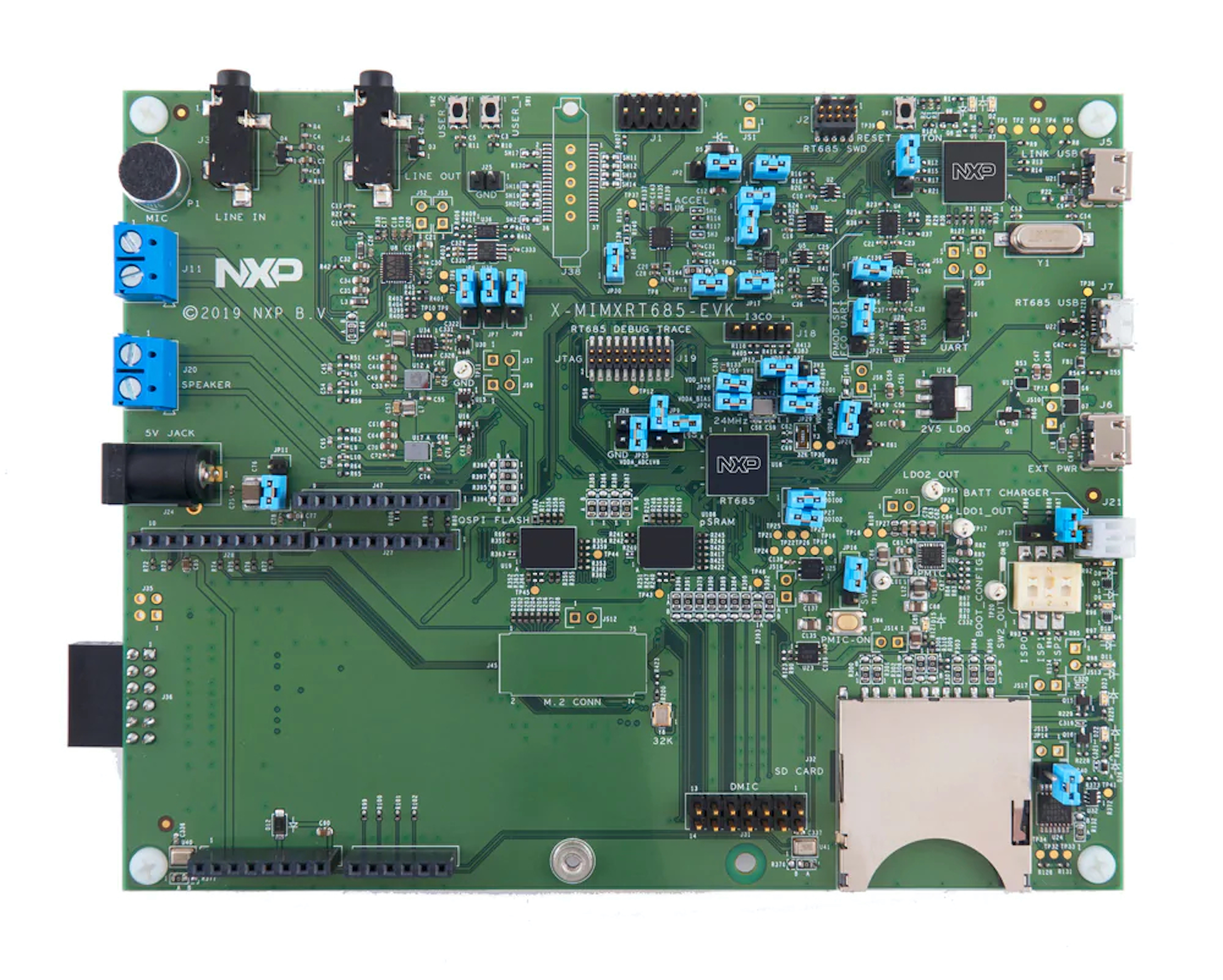
NXP’s i.MX RT600 development board (Image: NXP Semiconductors)
The i.MX RT600 multi-core crossover processor family features an Arm Cortex-M33 running up to 300 MHz and an optional Cadence Tensilica HiFi 4 audio/voice digital signal processor (DSP) running up to 600 MHz, with four MACS and hardware-based transcendental and activation functions.
Built on a 28-nm FD-SOI process optimized for active and leakage power, the i.MX RT600 supports the high-performance cores with 4.5 MB of on-chip low-leakage SRAM, which has been configured for simultaneous zero-wait state access, making it suited for real-time execution of audio/voice, ML, and neural network-based applications.
The crossover MCUs also feature EdgeLock, NXP’s advanced embedded security technology, and ML support using the eIQ for Glow neural network compiler.
Security features include secure boot with immutable hardware “root of trust,” SRAM physically unclonable function (PUF)-based unique key storage, certificate-based secure debug authentication, AES-256 and SHA2-256 acceleration, and DICE security standard implementation for secure cloud-to-edge communication. The chip also includes an optional fuse-based root key storage mechanism for secure boot and crypto operations and a public key infrastructure (PKI), or asymmetric cryptography, providing a dedicated asymmetric accelerator for ECC and RSA algorithms.
The crossover processors include an audio/voice subsystem with support of up to eight DMIC channels, with hardware for voice activation detect (VAD) and up to eight I2 S peripherals. Other peripherals include SDIO for wireless communication, high-speed USB with on-chip PHY, a 12-bit ADC with temperature sensor, and several serial interfaces including 50-Mbits/s SPI, I3C, and six configurable serial interfaces (USART, SPI, I2C, or I2S) with individual FIFO and DMA service request support.
NXP plans to implement the Ethos U-55 in its Cortex-M–based microcontrollers, crossover MCUs, and real-time subsystems in applications processors, targeting resource-constrained industrial and IoT edge devices.
The highly configurable Ethos-U55 machine-learning accelerator works with the Cortex-M core to achieve a small footprint, delivering greater than 30× improvement in inference performance compared to high-performing MCUs, said NXP.
Claimed as the first AI multicore processor for embedded sensor applications, Eta Compute Inc.’s ECM3532 neural sensor processor (NSP) features the company’s patented Continuous Voltage Frequency Scaling (CVFS) and delivers as low as 100-μW active power consumption in always-on applications. The ECM3532 multicore NSP combines an MCU and a DSP, both with CVFS, to optimize execution for the best efficiency, making it suited for IoT sensor nodes.
Designed for always-on image and sensor applications, Eta Compute’s NSP offers a complete software and hardware offering. The platform delivers AI to edge devices and turns sensor data into actionable information for applications such as voice, activity, gesture, sound, image, temperature, pressure, and biometrics. The platform solves challenges in edge computing, including lower response time, increased security, and higher accuracy.
The standalone AI platform includes a multicore processor, that includes flash memory, SRAM, I/O, peripherals, and a machine-learning software development platform. The CVFS substantially increases performance and efficiency for edge devices. The self-timed CVFS architecture automatically and continuously adjusts internal clock rate and supply voltage to maximize energy efficiency for the given workload. The ECM3532 is packaged in a 5 × 5-mm, 81-ball BGA.
Advertisement
Learn more about ARMMicrochip TechnologyNXP SemiconductorsRenesas Electronics AmericaSTMicroelectronics


