Innovations in image sensors are no longer centered around advancing camera performance in the mobile phone and digital camera markets. In the last year alone, there has been increased demand in better imaging for automotive safety applications, driven by advanced driver-assistance systems (ADAS) and automated driving, machine vision, security, 3D, and augmented and virtual reality (AR/VR). Here’s a sampling of some of those advances.
One of the leaders in the image sensor market is OmniVision Technologies Inc. The company recently claimed the first image sensor for automotive viewing cameras with 140-dB high dynamic range (HDR) and excellent LED flicker mitigation (LFM) for minimized motion artifacts. The OX03C10 CMOS ASIL-C automotive image sensor, with a large 3.0-micron pixel size, delivers 1,920 × 1,280p resolution at the highest rate of 60 frames per second (fps), which enables faster camera-view switching for drivers.
This is thanks to the company’s HALE (HDR and LFM engine) combination algorithm, Deep Well dual-conversion gain technology that provides much lower motion artifacts than other sensors with 140 dB, as well as split-pixel LFM technology with four captures. Basic image-processing capabilities like defect pixel correction and lens correction were also integrated into the sensor.
In addition, OmniVision’s PureCel Plus-S stacked architecture enables pixel performance advantages over non-stacked technology. The company cited a 20% improvement in the signal-to-noise ratio over the prior generation of its 2.5-megapixel (MP) viewing sensors thanks to 3D stacking that boosts pixel and dark current performance.
On top of these performance improvements, the OX03C10 also claims the smallest size, lowest power consumption, and best low-light performance for high-end viewing applications in premium vehicles. The OX03C10 achieves 25% lower power consumption than any LFM image sensor with 2.5-MP resolution, according to OmniVision, and when combined with the small package size, it enables the placement of cameras even in tight spaces. Automotive viewing applications include rearview cameras, surround view systems, camera monitoring systems, and e-mirrors. Available in both a-CSP and a-BGA packages, the OX03C10 image sensor is planned to be AEC-Q100 Grade 2-certified.
OmniVision also launched the first automotive-grade wafer-level camera module for driver monitoring systems (DMS). The OVM9284 1-MP CameraCubeChip module, measuring 6.5 × 6.5 mm, integrates the image sensor (3-micron pixel, ¼-in. optical format, 1,280 × 800 resolution), signal processor, and wafer-level optics in a single package to reduce design complexity and speed up development time.
The camera module’s small size, along with low power consumption — about 50% lower than competitors, according to OmniVision — enables DMS designers to fit the cameras in tight spaces and run continuously. In addition, it’s reflowable, meaning it can be mounted along with other components on the printed circuit board using automated surface-mount assembly equipment.
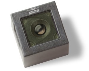
OmniVision’s OVM9284 1-MP CameraCubeChip module (Image: OmniVision Technologies Inc.)
There is also growing demand for 3D image sensors as more devices require context-based human-machine interaction. These sensors need to be small, energy-efficient, and highly reliable. One of the smallest, lowest-power-consumption 3D sensors for face authentication and photo effects on smartphones is available from Infineon Technologies AG.
Targeting smartphones and other 3D image data applications, Infineon, in collaboration with software and 3D time-of-flight (ToF) system specialist pmdtechnologies ag, has claimed the industry’s smallest and most powerful 3D image sensor. Introduced earlier this year, the REAL3 single-chip solution is Infineon’s fifth generation of ToF deep sensors. In addition to its small footprint of 4.4 × 5.1 mm, the chip provides the highest-resolution data with low power consumption.
Infineon’s deep sensor, or depth sensor ToF technology, enables an accurate 3D image of faces, hand details, or objects for applications that require exact matches to the original image as well as high reliability and security. One example cited is payment transactions using mobile phones or devices that don’t need bank details, bank cards, or cashiers, and the payment is carried out via facial recognition.
Key features include the capability to work in extreme lighting conditions, including bright sunlight and in the dark, and real-time full-3D mapping for AR experiences. The chip also provides additional options for camera applications such as enhanced auto-focus, bokeh effect for photo and video, and improved resolution in poor lighting. Infineon also offers an optimized illumination driver (IRS9100C) as part of a complete solution that further improves performance, size, and cost, said the company.

Infineon’s REAL3 3D image sensor (Image: Infineon Technologies AG)
For mobile 3D optical sensing systems, ams AG launched an ultra-sensitive near-infrared (NIR) image sensor that delivers a big advantage in power savings, enabling mobile device manufacturers to extend battery run time. The CGSS130 ¼-in. CMOS global shutter sensor (CGSS) is also said to be 4× more sensitive to NIR wavelengths than most other image sensors, reliably detecting reflections from very low-power IR emitters in 3D sensing systems.
The 1.3-MP stacked back-side illuminated (BSI) sensor offers a high quantum efficiency (QE), up to 40% at 940 nm and up to 58% at 850 nm. Thanks to the stacked BSI process used to fabricate the CGSS image sensors, they provide a small size — the die size is 3.8 × 4.2 mm and the GS pixel size is 2.7 µm.
The sensor produces monochrome images with a pixel array of 1,080 × 1,280 at a maximum frame rate of 120 fps. This high frame rate and global shutter operation produce clean images without blur or other motion artifacts, said ams. It also offers an HDR mode, achieving a dynamic range of more than 100 dB. Advanced functions include external triggering, windowing, and horizontal or vertical mirroring.
The CGSS130 NIR sensor enables high-performance depth maps for payment authentication, face recognition, and AR/VR applications. In addition to implementing face recognition in wearable devices and other products, powered by small batteries, the sensor also enables a new range of applications because the increased sensitivity extends the measurement range at the same power budget, said ams.
The company offers a full system solution — illumination, sensor, and software — to help mobile designers speed up development and differentiate their products. In addition to the NIR sensor, ams provides NIR VCSEL emitters and face-detection and face-matching software, along with reference designs for mobile 3D sensing.

The CGSS130 NIR sensor from ams (Image: ams AG)
Another new breed of image sensor is ON Semiconductor’s ARX3A0, enabling intelligent vision systems for viewing and AI. The company said the digital image sensor with 0.3-MP resolution in a 1:1 aspect ratio is the first of its kind designed for advanced and intelligent systems as well as traditional viewing systems. The ultra-small (1/10-in. optical format) and ultra-low-power ARX3A0 CMOS digital image sensor delivers high-performance image capture — even in low light — and minimal power consumption.
The image sensor consumes less than 19 mW when capturing images at 30 fps and 2.5 mW when capturing 1 fps. It also features advanced power management capabilities, such as automatically waking from a low-power mode when detecting motion or lighting changes in the scene. This allows the sensor to become the main source of wake for the camera system, saving additional system power.
The ARX3A0 can capture 360 fps, similar to a global shutter with the size, performance, and responsivity of a BSI rolling shutter sensor. Thanks to its small size, square form factor, and high frame rate, the image sensor can be used in machine vision, AI, and AR/VR applications, as well as supplemental security cameras. One application example is AR/VR googles to monitor the wearer’s eye movements to help adjust the image viewed. In this application, the 1/10-in. square format enables low-height modules, while the 3.5-mm die size helps maximize the sensor’s field of view.
The monochrome sensor is based on a 560 × 560 active-pixel array that features ON Semiconductor’s NIR+ technology. This gives the image sensor high sensitivity at near IR wavelengths to deliver excellent performance in no light or when lighting is used that is non-detectable by the human eye, said ON Semiconductor.
The ARX3A0 is available in both chip-scale package and reconstructed wafer die. Evaluation boards running on ON Semiconductor’s PC-based DevWare system and prototype modules are available.
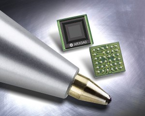
ON Semiconductor’s ARX3A0 digital image sensor (Image: ON Semiconductor)
SmartSens Technology recently expanded its AI Smart Sensor family with the introduction of the SC500AI 5-MP widescreen smart image sensor for security video and surveillance applications. The company said the next-generation sensor solves the challenge of most 5-MP security camera sensors with a 4:3 aspect ratio that are not optimized for modern widescreen-format LCD displays.
The SmartSens SC500AI fixes this problem with a 1,620p 16:9 5-MP video output in the same form factor. Thanks to the company’s SmartClarity technology, it increases the number of pixels by 20% compared with many 5-MP products on the market. This leverages the full resolution of the sensor rather than cropping a 5-MP 4:3 image down to 4 MP to fit a 16:9 aspect ratio, which reduces dark edges and distortion on both sides of the image to achieve a true 16:9 aspect ratio that includes an additional 10% of horizontal viewing area, said SmartSens.
Compared with SmartSens’s previous-generation sensor, the new SC500AI reduces the dark current from 389 e– at 80˚C to 210 e–. The total read noise (RN) is reduced from 0.75e– to 0.63e–, and the sensitivity level also improves from 2,800 mV/lux-sec to 3,680 mV/lux-sec.
These improvements are attributed to SmartSens’s SFCPixel technology that increases the sensitivity level for high-quality night-vision images. In addition, the company’s proprietary PixGain technology enables the sensor to achieve excellent HDR performance even in glaring sunlight.
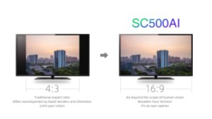
SmartSens’s SC500AI smart image sensor (Image: SmartSens Technology)
Aimed at enabling the next generation of smart computer-vision applications with high-speed, global-shutter image sensors — preferred for capturing distortion-free images when the scene is moving or when NIR illumination is needed — are the new NIR-optimized VD55G0 (captures up to 210 fps in a 640 × 600 pixel resolution) and VD56G3 with 1.5-MP (captures up to 98 fps in a 1,124 × 1,364 pixel resolution) sensors from STMicroelectronics.
The company claims the VD55G0 and VD56G3 sensors, measuring 2.6 × 2.5 mm and 3.6 × 4.3 mm, respectively, are the smallest on the market in relation to resolution. They also tout low pixel-to-pixel crosstalk at all wavelengths, specifically near-infrared, delivering high contrast for superior image clarity. These sensors are optimized for better object detection and recognition for 2D and 3D sensing. Applications include AR/VR, simultaneous localization and mapping (SLAM), and 3D scanning.
ST attributes the pixel size, high sensitivity, and low crosstalk of the sensors to its image-sensor process technologies — a combination of silicon process innovation and advanced pixel architecture that allows a smaller sensor pixel array on the top die while keeping more silicon area on the bottom die to increase digital-processing capabilities and features.
The advanced pixel technology, including full Deep Trench Isolation (DTI), enables extremely small 2.61 × 2.61-μm pixels that combine low parasitic light sensitivity, high QE, and low crosstalk in a single die layer. In addition, ST’s approach allows for a small pixel on the BSI die for space-saving vertical stacking of the optical sensor and related signal-processing circuitry on the bottom die for a very small sensor size and more features.
The bottom die is fabricated in ST’s 40-nm technology and integrates digital and analog circuitry. The digital circuitry incorporates hardware features including an exposure algorithm with statistics gathered from up to 336 zones, automatic defect correction, and automatic dark calibration.
The fully autonomous low-power optical-flow block can calculate 2,000 movement vectors at 60 fps. The embedded vector generation delivers advantages in AR/VR or robotics to support SLAM or six-degrees-of-freedom (6DoF) use cases, especially in host systems with limited processing capabilities, said ST.
The sensors support multiple frame contexts with programmable sequencing, including full illumination controls. Other features include an integrated temperature sensor, I2C Fast mode+ control, defect correction, windowing, binning, and MIPI CSI-2 data interface.
Sony Corp. has also advanced global shutter image sensor technology with the recently released IMX990 and IMX991 compact short-wavelength infrared (SWIR) image sensors for industrial equipment. These sensors can capture images across both the visible and invisible light spectrums in the short-wavelength infrared range and deliver a compact size with the smallest 5-μm pixel size, based on SWIR image sensors using indium gallium arsenide (InGaAs). Targeting the development of SWIR industrial cameras and inspection equipment for a range of applications such as inspection, identification, and measurement, IMX990 and IMX991 global shutter sensors overcome challenges in pixel miniaturization to deliver compact and high resolution from the visible spectrum to SWIR wavelengths.
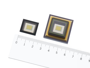
Sony’s IMX990 and IMX991 SWIR image sensors (Image: Sony Corp.)
The SWIR image sensors’ high sensitivity over a broad range of wavelengths, from 0.4 μm to 1.7 μm, is thanks to Sony’s SenSWIR technology, in which photodiodes are formed on an InGaAs compound semiconductor layer and are connected via Cu-Cu connection with the silicon layer, which forms the readout circuit. This opens up new opportunities for the development of cameras and testing equipment in a variety of applications.
The new products also support digital output, matching the performance of current CMOS image sensors for industrial equipment, allowing for many features and functionality. This reduces the number of steps in camera development and makes multifunction camera development easier, said Sony.
The smaller pixel pitch made possible by the Cu-Cu connection, resulting in the 5-μm pixel size, makes it possible to reduce camera size while maintaining SXGA (IMX990)/VGA (IMX991) resolution, contributing to improved testing precision, said Sony. Both devices are available in a ceramic LGA package and ceramic PGA package with a built-in thermoelectric cooler.
Innovation also continues for cameras in smartphones. Samsung Electronics recently introduced the ISOCELL camera sensor with 50-MP resolution with larger pixels, faster DSLR-level auto-focus speeds, brighter images, and 8K video recording. The ISOCELL GN1 with 1.2-μm pixels is the company’s first image sensor to offer both Dual Pixel auto-focus and Tetracell pixel binning technologies, addressing various imaging user preferences, for extremely detailed images with ultra-high resolution or bigger pixels for brighter images in low-light environments.

Samsung’s ISOCELL GN1 camera sensor (Image: Samsung Electronics)
The GN1 delivers best-in-class auto-focusing with 100 million phase-detection auto-focus (PDAF) agents. The Dual Pixel technology places two photodiodes side by side within a single pixel that can receive light from different angles for phase detection. When capturing images, a single pixel output is created by merging the outputs from the two photodiodes within the pixel. A software algorithm takes the light information from each photodiode to produce image resolutions comparable to 100 MP.
Samsung also said the ISOCELL GN1 can provide 2.4-μm pixels using the Tetracell technology for “ultimate” low-light photos. The Tetracell technology is a pixel-merging technique that improves the pixels’ capacity to capture and process more light. By binning four pixel signals into one, Tetracell doubles the image sensor’s pixel size to 2.4 μm and quadruples the light sensitivity to take brighter 12.5-MP images.
Other features include Smart-ISO that intelligently selects the optimal ISO, real-time HDR that captures the scene in multiple exposures simultaneously, and gyro-based electronic image stabilization that takes sharp images and video even when in motion. The image sensor supports video recording at up to 8K resolution at 30 fps.
Advertisement
Learn more about ams (formerly austriamicrosystems)Infineon TechnologiesOmniVision TechnologiesON SemiconductorSamsung ElectronicsSmartSens TechnologySonySTMicroelectronics