Performance requirements from industrial automation and industrial IoT (IIoT) designers continue to change. Their wish list includes microcontrollers (MCUs) with faster processing, more memory, improved connectivity, and more security features. MCU manufacturers are listening, and the result is a new breed of microcontroller that offers designers a balance of performance, security, and cost.
“With the Industrial automation market moving towards Industrial 4.0 or IIoT, there are more interconnected sensors, instruments, and other devices networked together for data collection and analysis purposes to improve the productivity and efficiency for manufacturing plants. As such, there is increasingly more requirement for more connectivity features in the network,” said Mamoru Sakugawa, director, IoT Platform Business Division, Renesas Electronics. “Due to the different requirement and targeting different aspect of the sensors/network, different communication protocols (i.e. EtherNet/IP, PROFINET etc) are used and there is no single one that dominates in the market now.”
“This drives the need for a higher processing power to interconnect all the devices seamlessly with no lag in the communication. With more communication in the network, the requirement for higher security in the network is also getting important,” he added. “All this again will drive down to the need for more embedded memory and SRAM within the system.”
IIoT also is driving its own set of unique requirements around measurement and control, while requiring a balance between performance and cost.
“IoT continues to become more widespread, both as a data communication system and as a buzzword. In industrial settings, the growth of IoT is visible as an increasing number of distributed nodes with various amounts of autonomy to measure and control parts of processes,” said Steve Kennelly, senior manager, Medical Products, MCU8 business unit, Microchip Technology. “Besides the ability to communicate via one or more protocols, these nodes need to reach an economically-appropriate level of independent real-time control capability.”
Kennelly said successful implementations must balance performance, which is usually realized as a deterministic response with minimum latency, with cost that needs to be low enough to enable the scaling that IoT implies. “New microcontrollers are changing the relationship between the CPU core and peripherals by redefining peripherals as easily configurable hardware blocks. This allows very cost-effective platforms that can react to inputs in less time than a CPU instruction cycle.”
Microchip’s AVR DA family of MCUs is an example of the new breed of MCUs that changes the balance of cost and performance in IIoT applications, said Kennelly. “It combines the popular 8-bit AVR microcontroller core with core-independent peripherals that can operate autonomously after being configured in software.
“The Event System connects multiple peripherals so that changes in one can trigger actions in others without CPU intervention,” he said. “This allows the creation of functional blocks that are fully deterministic and much faster than is possible by executing code. Functions such as arbitrary signal generation, analog signal filtering, custom communication protocols, and many more can easily be created with graphical tools.”
Kennelly said a small node, like an intelligent sensor that gathers data and sends periodic data packets over a network could be realized in a single-chip design using the AVR DA MCU. “In more complex systems, for example where each node is a small Linux computer, the AVR DA could be dedicated to certain functions that require fast, deterministic response.”

Microchip’s AVR DA family of MCUs (Image: Microchip Technology)
The AVR DA family of MCUs also is Microchip’s first functional safety ready AVR MCU family with peripheral touch controller (PTC), enabling real-time control, connectivity, and human machine interface (HMI) applications. Microchip’s Functional Safety Ready designation is applied to devices that incorporate the latest safety features and are supported by safety manuals, failure modes, effects, and diagnostic analysis (FMEDA) reports, and in some cases, diagnostic software.
“As functional safety is becoming mandatory in a growing number of industrial applications, the AVR DA is also the first AVR MCU to be introduced to the market with a suite of resources to support certification efforts to a number of standards,” said Kennelly.
The AVR DA MCUs enable CPU speeds of 24 MHz over the full supply voltage range, memory density of up to 128 KB flash, 16 KB SRAM and 512 bytes of EEPROM, 12-bit differential ADC, 10-bit DAC, analog comparators, and zero cross detectors. The PTC enables capacitive touch interface designs supporting buttons, sliders, wheels, touchpads, smaller touch screens as well as gesture controls for a variety of consumer and industrial products and vehicles. It supports up to 46 self-capacitance and 529 mutual capacitive touch channels and features the latest generation PTC with Driven Shield+ and boost mode technologies providing, enhanced noise immunity, water tolerance, touch sensitivity, and response time.
Security matters
While performance is a big factor in the selection of MCUs, device security has become a big concern for industrial OEM designers.
“To have truly secure processor platforms, the processor not only must protect the IPs from the silicon level, but it must have the capability to ensure protection against threats throughout the lifecycle of an IoT device,” said Sakugawa. “Simply put, it must be managed in different stages of an IoT device lifecycle, called device lifecycle management (DLM), starting from design to manufacturing, out in the market, field firmware upgrade to end of life of the product. Each stage needs to have security implemented to ensure information is not leaked.”
Is silicon the first line of defense when it comes to device security? “The first level will always have to come from system implementation, that is the IoT device itself,” said Sakugawa. “If the system is not implemented properly, it is then open to vulnerable threats and a potential threat to the silicon level, which should be the final line of defense. Therefore, security implementation is not just about silicon-level implementation only.”
Kris Ardis, executive director for the Micros, Security and Software Business Unit at Maxim Integrated said the first line of defense has to come from awareness.
“The first line of defense is awareness of the threats an application may come up against,” said Ardis. “While I strongly believe that security should start in the silicon as a root of trust for any embedded application, even my most secure microcontroller won’t help if the implementer doesn’t consider the threats and unintentionally leaves backdoors open.
“While Maxim Integrated has always promoted highly secure solutions due to our background providing financial and government-grade security solutions, it wasn’t until the last few years with well-publicized attacks like Mirai and Stuxnet that we started to see a pull from our customers,” said Ardis. “We integrate proven crypto engines, secure bootload technology, and high quality random number generators into most of our micros for the industrial and medical markets.
“The IoT really hints at distributed devices that aren’t tethered to the wall — this makes them more attractive targets to attackers. Carrying out a successful attack is always about risk —if a device can easily be stolen, then there is little risk to an attacker getting physical access,” said Ardis.
“This means that we need to be much more concerned with the ability of an attacker to do things like extract code or secret key information,” he added. “In higher value applications, we may even see active tamper detection technology employed to erase sensitive information if the application senses someone is trying to break into it.”
But best-in-class security features will depend on the application. “Products in the financial terminal space offer very advanced security features — low power, always-on sensors monitor for many kinds of attacks. Other technology like PUF [Maxim Integrated provides an implementation of physical unclonable function (PUF) called ChipDNA] helps to provide superior secret key protection without a battery,” said Ardis.
These technologies do incur a cost, but there are plenty of other technologies that can help keep out a wide array of attackers, said Ardis. “A good secure boot methodology can frustrate many attackers and keep your IP safe from alteration or discovery.”
Performance + security
Maxim Integrated also recently starting to introduce error-correcting-code (ECC) technologies in their microcontrollers to enhance reliability. “As our embedded microcontrollers go down in process technology, the memories (in particular SRAMs) are more susceptible to disturbance from energy particles. Effective use of ECC can take the failure rates from 1 bit failure per some number of months to 1 failure per number of centuries,” said Ardis.
“We’re also seeing a push for more capable microcontrollers — more memory means more complex decisions can be made at the edge, lessening the demand for wireless or wired communication which is already capacity constrained in many environments and always much higher power than making the decision locally,” he said.
Maxim Integrated’s MAX32670 low-power Arm Cortex-M4 MCU is an example that delivers on both performance and security. The MCU includes ECC-protected memory, a secure bootloader, and crypto support to help IoT and industrial applications meet long lifetimes in harsh environments and under extreme power constraints.
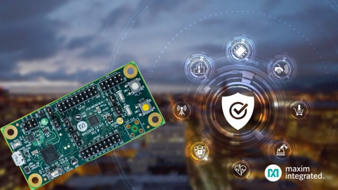
Maxim Integrated’s MAX32670 low-power Arm Cortex-M4 MCU (Image: Maxim Integrated)
In addition to the integrated ECC-protected memory, the MAX32670 offers low-power consumption and a small size, delivering a 40% power savings and 50% space savings. Designed for industrial, health-care, and IoT sensor applications, the MCU delivers just 40 µW/MHz of active power consumption, making it the lowest power solution for battery-operated sensor applications, said Microchip, and is 50 percent smaller than the closest competitor, in ultra-small 1.8 × 2.6-mm WLP and 5 × 5-mm TQFN packages.
The MAX32670 protects the entire memory footprint (384 kB flash and 128 kB SRAM) with ECC to prevent bit flips and to enhance reliability. “Bit flipping becomes a critical reliability concern as microcontrollers scale down to 40 nm and below,” said Ardis. “With ECC, single-bit errors are detected and corrected by hardware, making it difficult for bit flip errors to have a negative impact on the application.”
Another MCU family that balances functionality with security are the 32-bit RX72N and RX66N MCUs from Renesas Electronics. Aimed at industrial automation applications, the MCUs combine equipment control and networking function on a single chip, along with functionality improvements, and security features.
For industrial IoT and industrial automation, Renesas looks at three areas – real-time performance, multi-functionality combined with miniaturization of industrial equipment, and industrial network support, said Sakugawa.
In the industrial equipment market, performance and functionality improvements lead to larger program code sizes. As a result, memory storage capacity and read speed play a key role in determining real-time performance,” he said.
“In recent years, most products for industrial automation are connected to networks and installed many functions like LCD panels. However, in many cases, additional MCUs and memory are necessary to support network connectivity or additional functions without sacrificing key features,” he said.
“On the other hand, there is a need for miniaturization of equipment, and conflicting demands are becoming a challenge in designing new equipment. It is important for processors on a single chip to minimize the BOM [bill of materials] by having a higher performance processor for multi-tasking, higher embedded memory, I/O pins, and other key peripheral functions to realize it.”
The Renesas MCUs are built around the company’s RXv3 CPU core with 5.82CoreMark/MHz. The RX72N features a maximum operating frequency of 240 MHz with 1396CoreMark and two Ethernet channels, while the RX66N offers a 120-MHz maximum operating frequency with 698CoreMark, and one Ethernet channel.
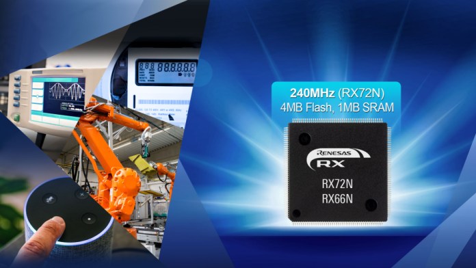
Renesas Electronics’ 32-bit RX72N and RX66N MCUs (Image: Renesas Electronics)
The devices offer up to 4 MB of on-chip flash memory that perform read operations at a frequency of 120 MHz, among the fastest in the industry, as well as 1 MB of on-chip SRAM. This on-chip memory eliminates the need for external memory, which has slower read speeds, and makes it possible to extract the full performance capacity of the CPU. The larger memory capacity also enables high-resolution graphics support, such as WVGA, on a single chip, which was not possible on earlier general-purpose MCUs.
“The RX72N, and RX66N products have the industrial largest capacity of memory with 4 MB of flash memory and 1 MB of SRAM. This ensures enough space for user applications as well as data that was previously stored in external flash memory, such as LCD image data,” said Sakugawa. “Utilizing the large amount of SRAM and processing the LCD image data in a two-layer configuration enables smooth display performance.
“These products are also available in packages with up to 224 pins. This enables many features to be implemented without the need for external memory or a sub-MCU, which results in better performance over previous products, while also contributing to a reduction in the number of components, size of circuit boards, and development time,” he added.
The MCUs can implement single-chip equipment control and networking function, enhancing the real-time performance of applications such as industrial robots, general-purpose inverters, programmable logic controllers (PLCs), and remote I/O devices.
The devices also incorporate a hardware accelerator for fast motion control. The arithmetic unit for trigonometric functions (sin, cos, arctan, hypot; RX72N only) accelerates motor vector control and a register bank save function that decreases the interrupt response time. This reduces the CPU load required for closed-loop control and simplifies the implementation of additional functions such as networking capabilities.
The MCUs also incorporate an LCD controller, 2D drawing engine, and serial sound interface. They can support high-resolution displays — WVGA (800 × 480) at 8-bit colors or WQVGA (400 × 240) at 16-bit colors — without the need for external memory. When used in combination with voice recognition or noise reduction middleware, they also enable customers to add voice control function to their products, making them well suited for applications such as network-connected LCD-equipped controllers or smart speakers.
Addressing the security aspect, the MCUs also come with a high-security IP – Trusted Secure IP (TSIP) that supports many cryptographic engines and key management to prevent the MCU from being tampered and hacked into through the network, said Sakugawa.
The Trusted Secure IP module is provided as a security engine to support multiple encryption standards, including AES, 3DES, RSA, ECC, SHA, and TRNG, as well as key management. Combined with the protection function of the on-chip flash memory, it provides support for secure firmware updating and secure boot function.
“In any implementation, the security of a system will always be driven from its root and in this case the brain of the system, which stores the processing algorithm and important data. Losing control of this means losing control of the whole system. This is the reason why security has to start from the silicon level. If your silicon is vulnerable to threats, you simply will lose the whole control of your system,” said Sakugawa.
“In the RX Trusted Secure IP, there is a 128-bit unique ID and TRNG that allows keys to be generated securely and managed within the TSIP,” he added. “The TSIP is also certified by the NIST CAVP [Cryptographic Algorithm Validation Program] program for a truly secure algorithm that realizes the root of trust within the silicon.”
In addition, IAR Systems released new versions of its security development tool C-Trust and the Security from Inception Suite, which extends device support for a number of Renesas MCUs, including the RA and RX MCU families. Support is now extended to the RX72N.
C-Trust is an extension of the IAR Embedded Workbench and enables developers to protect an existing or new application without having to master security complexities. It provides protection against IP theft, malware injection, counterfeiting, and overproduction.
The Security from Inception Suite for implementing and customizing security in embedded applications integrates C-Trust with additional security development tools plus training to support companies that need to meet legislative requirements, such as California and Oregon consumer laws, the ETSI TS 103 645 standard, and the IEC 62443 industrial IoT security standard.
Another MCU that addresses security demands and high performance requirements for IoT is the STMicroelectronics ultra-low-power STM32L5x2 MCUs to better protect IoT-connected applications. These controllers offer proprietary security built on Arm TrustZone technology (and is PSA Certified Level 2), along with secure boot, full hardware isolation, and crypto accelerators.
The security foundation of the STM32L5 MCUs, operating at clock frequencies to 110 MHz, starts with the Arm TrustZone hardware-based security. Designers can include or exclude each I/O, peripheral, or area of Flash or SRAM from TrustZone protection, which allows sensitive workloads to be fully isolated for maximum security, said ST.
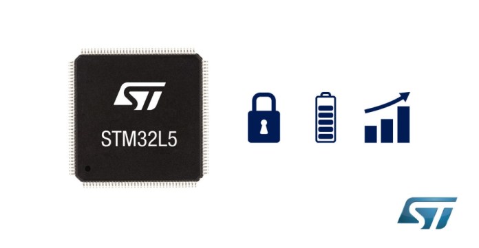
STMicrolectronics ultra-low-power STM32L5x2 MCUs (Image: STMicroelectronics)
The company said it has engineered TrustZone to ensure support for secure boot, special read-out and write protection for integrated SRAM and Flash, and cryptographic acceleration, including AES 128/256-bit key hardware acceleration, public key acceleration (PKA), and AES-128 On-The-Fly Decryption (OTFDEC), to protect external code or data. The STM32L5 also supports active tamper detection and secure firmware installation.
The company also offers designers a consolidated and comprehensive toolset of cyber-protection resources for IoT designs, called STM32Trust. Tools, evaluated reference material, and source code can be downloaded for free.
ST doesn’t ignore the need for lower power consumption in IoT applications. The STM32L5 incorporates techniques such as adaptive voltage scaling, real-time acceleration, power gating, and multiple reduced-power operating modes to enable the MCUs to deliver high performance and long run-times, whether powered by coin cells or even through energy harvesting. In addition, a highly efficient switched-mode step-down regulator can be powered up or down on-the-fly to improve low-power performance when the VDD voltage is high enough.
In addition, the STM32L5x2 MCUs offer 512 Kbyte dual-bank Flash that allows read-while-write operation to aid device management and supports ECC with diagnostics. There is also a 256 Kbyte SRAM and features to support high-speed external memory including single, dual, quad, or octal SPI and Hyperbus Flash or SRAM, and an interface for SRAM, PSRAM, NOR, NAND or FRAM.
Advertisement
Learn more about Maxim IntegratedMicrochip TechnologyRenesas Electronics AmericaSTMicroelectronics


