
Modern ICs involve more than monolithic silicon; they blend multiple chips from different silicon process technologies mounted on varying substrates and housed in a variety of package types. Traditional chip design tools, however, do not accommodate the effect of packaging and require manual corrections when validating design performance. Cadence’s Virtuoso System Design Platform integrates IC design and package analysis to enable concurrent design across chip, package, and board.
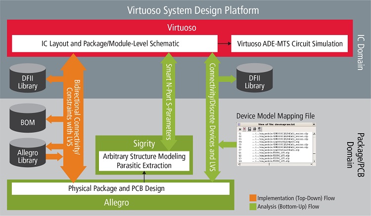
The platform blends Cadence’s Virtuoso Schematic Editor and Analog Design Environment into a unified tool for design capture, analysis, and verification at the chip, package, and board levels. In addition, the platform offers an automatic, bidirectional link to a system-in-package (SiP) implementation environment and to the Sigrity 3D electromagnetic modeling system. The combination gives chip developers the ability to work with a single, system-aware schematic that automatically incorporates all the parasitic and electromagnetic effects that the finished, packaged design will face.
Because the platform automates the inclusion of packaging and board-level effects, it eliminates the currently manual process of adding those effects to the IC’s layout model when simulating chip performance. This automation both speeds the design flow from days to minutes and eliminates the errors generated when using manual entry of package parametric information from spreadsheets and other ad hoc sources. These enhancements improve the alignment of the platform with the demands of modern SiP designs.
Advertisement
Learn more about Cadence Design Systems