Microelectromechanical systems (MEMS) present both unique market opportunities and significant manufacturing challenges for product designers in nearly every application segment. Used as accelerometers, pressure sensors, optical devices, microfluidic devices, and more, these microfabricated sensors and actuators often need to be exposed to the environment, but also need to be protected from environmental factors. Although standard semiconductor manufacturing methods provide a baseline capability in meeting these challenges, the unique requirements of MEMS devices drive a need for specialized epoxies and adhesives able to satisfy often-conflicting demands.
Built with processing steps similar to IC fabrication, MEMS devices range in size from several millimeters to less than a micron and can vary in function from simple static structures to complex systems with moving elements (fig.1 ). At the dimensions of MEMS structures, physical effects such as static friction (stiction) arise due to the extremely close spacing of micromachined elements. Along with internal effects, external conditions such as temperature, humidity, and particulate contamination can damage devices or impact their long-term reliability. In fact, as with any mechanical device, corrosion and wear can degrade performance over time.
Fig. 1: MEMS structures, such as this vibrating cantilever, dictate use of specialized packaging methods and materials to ensure function and long-term reliability. (Source: Pcflet01 at en.wikipedia)
Reliable die attach
Individual MEMS die are attached to a metal, ceramic, or plastic package using IC-manufacturing die-attach methods to provide mechanical support as well as thermal and electrical conductivity between the die and package base. Although eutectic alloys such as gold or gold/tin have been used in IC manufacturing to solder dies onto packages, the high process temperatures used in this method create large stresses from mismatches between the coefficient of thermal expansion (CTE) of the silicon die and the package base material. Consequently, MEMS device manufacturers typically use epoxies, Such as those supplied by Master Bond (www.masterbond.com) and others) which are typically stronger and less affected by process variation. Furthermore, the specific characteristics of these epoxies can be enhanced by adding fillers such as silica for insulation or silver for conduction, hardeners to enhance strength, catalysts to speed curing, and other materials to optimize specific properties such as CTE, moisture uptake, adhesion, and dispersal.
After the die is placed, the epoxy must be cured to fix it in place using cure methods that typically trade lower temperature for higher cure time. In fact, engineers can find different epoxies and even cure methods that yield the specific die attach strength, resistivity, and thermal conductivity required for each specific MEMS device, package, and application. For example, a relatively low temperature cure cycle may be needed to protect materials such as anti-stiction coatings on the MEMS device.
The selection of both a particular epoxy and an effective curing process are critical in maintaining the integrity and long-term reliability of MEMS devices. As with any die-attach methods, epoxy bonds can fail unless the manufacturer takes sufficient care to ensure complete coverage of the material in the bonding area between the die and package. Variations in process temperature can affect epoxy viscosity, and increased temperatures can cause solvent contaminants to migrate across the affected surface. Furthermore, use of epoxies that have exceeded the recommended shelf life can result in contamination of the bond, leading to decreased conductivity and possible loss of adhesion. Finally, different materials exhibit different aging characteristics. In the worst case, aging can result in breakdown of the die-attach bond.
Enhanced reliability with underfill
Flip-chip manufacturing has gained widespread adoption due to its performance, size, and I/O density advantages over conventional packaging. In fact, flip-chips allows use of nearly the entire chip surface for interconnect, eliminating the disproportionate amount of die real estate required in the past for interconnect pads while providing a level of package miniaturization of particular interest to MEMS manufacturers.
A key step in flip-chip manufacturing includes filling the tiny space between the chip and substrate with epoxy to further enhance reliability. After curing, this epoxy “underfill” strengthens the mechanical coupling between the die and the package, minimizes moisture absorption, and helps relieve any CTE mismatch, thus improving the reliability of the joints and overall assembly.
A critical characteristic of the underfill lies in its ability to provide a favorable CTE match with the solder bumps that used to interconnect the chip and substrate. A good CTE match reduces thermal stresses on solder joints by redistributing those stresses more uniformly across solder joints, chip, substrate, and underfill itself. In fact, manufacturers have found that use of the proper underfill material increases the thermal-cycling lifetime of solder joints by more than an order of magnitude.
For all its advantages, underfill can actually introduce problems unless it is selected with careful attention to its physical properties. For example, underfill material is typically dispensed by injection and drawn into the tiny spaces between flip-chip and package through capillary action. As it fills, the material needs to possess the appropriate viscosity to avoid creation of voids, which create points of high stress that may lead to early delamination. Once in place, the material requires sufficient shear and tensile strength to resist formation of microcracks, which can expand with thermal cycling and lead to early chip failure. Furthermore, underfill material that shrinks during curing can induce stresses large enough to crack the die itself.
Similar concerns arise during the end-product life cycle. Underfill materials that age prematurely due to thermal cycling or environmental conditions can contribute to delamination and product failure. In fact, continued exposure to high humidity can lead to swelling of underfill materials that exhibit poor moisture absorption properties, leading to additional stress within the packaged MEMS device and likely failure.
Specialized encapsulation
For MEMS manufacturers, balancing the need to protect these devices while still allowing them to interact with the environment gives rise to specialized methods for encapsulating the MEMS device, integrated electronics circuits, and wire bonds. For example, MEMS pressure sensors are buried in cavities built during fabrication or enclosed by walls added during packaging and finally covered with a membrane.
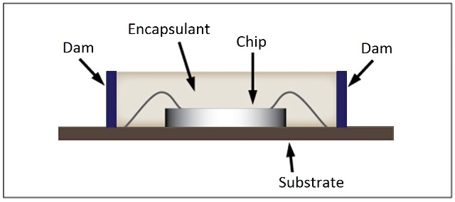
Fig. 2: Using dam-and-fill techniques, manufacturers use high-viscosity materials to build dams, which create a well around the MEMS chip, and then fill it with low-viscosity materials to completely encapsulate the entire assembly. (Source: Master Bond Inc.)
For MEMS chips, encapsulation often relies on conventional “dam-and-fill” techniques (fig. 2 ). Depending on the MEMS device and application, the well is filled with a lower-viscosity material that creates a thin layer over the die and around the wire bonds. The dam created by the ring of high-viscosity material allows use of a thinner material able to flow quickly and smoothly to complete the fill process faster while achieving the uniformity required to ensure encapsulation of the assembly.
Advertisement
Learn more about Master Bond


