By Gina Roos, editor-in-chief
Researchers at the Georgia Institute of Technology have developed a bonding technique that addresses the challenge of heat dissipation in high-power electronics applications using wide-bandgap (WBG) materials like gallium nitride (GaN) in miniaturized devices. This technique, which can improve the cooling of GaN devices, could be used in high-power and high-frequency electronic devices including wireless transmitters, radars, and satellite equipment.
The adoption of WBG materials continues to grow in the power electronics industry thanks to their high-efficiency, high-power, and high-temperature advantages. Compared with traditional silicon processes, WBG semiconductors enable better thermal conductivity, higher switching speeds, and smaller footprints to deliver a new generation of power devices.

(Image: Yole)
But like many new technologies gearing up for widespread adoption, there are always design challenges. In high-power applications using materials such as GaN in miniaturized devices, heat dissipation can limit power density.
Today, engineers use a layer of diamond, which conducts heat 5× better than copper, to try to spread and dissipate the thermal energy. The problem is that when diamond films are grown on GaN, they need to be seeded with nanocrystalline particles that measure about 30 nm in diameter, resulting in a layer of nanocrystalline diamond that has low conductivity, said researchers. In addition, the growth is done at high temperatures, which can cause thermal stress and damage the devices.
Addressing these challenges, the research team has developed a room-temperature bonding technique, called surface-activated bonding, for integrating GaN with thermally conducting materials such as diamond. This creates a thinner interface, which moves the thermal dissipation closer to the GaN heat source for better cooling and higher performance. This could result in higher power levels, longer device lifetime, improved reliability, and reduced manufacturing costs, according to the researchers.
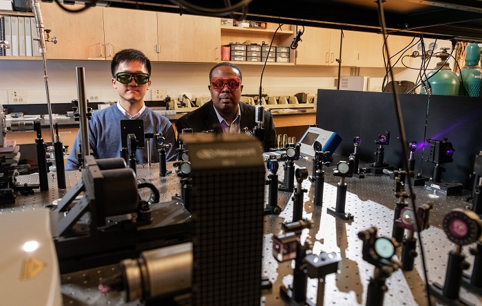
Researchers Cheng Zhe and Samuel Graham are shown with an optical test setup for studying GaN devices cooled by placement on a diamond substrate. (Image: Rob Felt, Georgia Tech)
This technique allows the high thermal conductivity materials to be placed much closer to the active device regions in gallium nitride, according to Samuel Graham, the Eugene C. Gwaltney Jr. School Chair and professor in Georgia Tech’s George W. Woodruff School of Mechanical Engineering. “The performance allows us to maximize the performance for gallium nitride on diamond systems,” he said. “This will allow engineers to custom-design future semiconductors for better multi-functional operation.
“In the currently used growth technique, you don’t really reach the high thermal conductivity properties of the microcrystalline diamond layer until you are a few microns away from the interface,” he explained. “The materials near the interface just don’t have good thermal properties. This bonding technique allows us to start with ultra-high thermal conductivity diamond right at the interface.”
How it works: The surface-activated bonding uses an ion source in a high-vacuum environment to clean the surfaces of the GaN and diamond, which activates the surfaces by creating dangling bonds, said the researchers. Then small amounts of silicon are introduced into the ion beams to form strong atomic bonds at room temperature. This allows the direct bonding of the GaN and single-crystal diamond to fabricate high-electron-mobility transistors (HEMTs).
The result is a 4-nm-thick interface layer from GaN to single-crystal diamond, which enables up to 2× more efficient heat dissipation than in state-of-the-art GaN-on-diamond HEMTs.
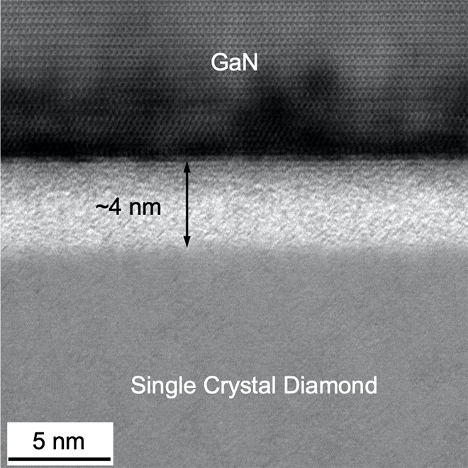
Diamond-interface: cross-section bright-field high-resolution STEM images of GaN-diamond interfaces using the surface-activated bonding technique. (Image: Zhe Cheng, Georgia Tech)
In addition, the room-temperature process reduces the thermal stress from as much as 900 megapascals (MPa) to less than 100 MPa. “This low-stress bonding allows for thick layers of diamond to be integrated with the GaN and provides a method for diamond integration with other semiconductor materials,” said Graham.
Researchers said that this process will allow them to mix and match materials and optimize for electrical, thermal, and mechanical properties. But the real advantage is “a vastly superior thermal interface,” said Graham.
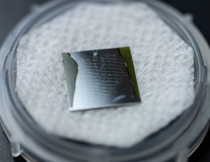
Polished GaN-SiC samples bonded by the surface-activated bonding technique. (Image: Rob Felt, Georgia Tech)
This new technique can be used with other semiconductors, such as gallium oxide, and other thermal conductors, such as silicon carbide. Researchers plan to evaluate other ion sources and materials that can be used with the technique.
The research, conducted in collaboration with scientists from Meisei University and Waseda University in Japan, was reported in the journal ACS Applied Materials and Interfaces. The work was supported by a multidisciplinary university research initiative (MURI) project from the U.S. Office of Naval Research (ONR).
Advertisement
Learn more about Electronic Products Magazine